AD102, AD103 and AD104: transistors, number of cores and more on the GPUs of the early GeForce RTX 4000
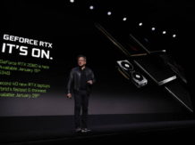
NVIDIA announced early on that the first three video cards of the GeForce RTX 4000 era are based on three distinct GPUs: AD102 for the RTX 4090, AD103 for the RTX 4080 16 GB and AD104 for the RTX 4080 12 GB.
However, the company had not shared many technical details, especially with regard to AD103 and AD104, leaving us with a poorly defined technical framework. Now, thanks to sharing a whitepaper, we have one complete view of the characteristics of the GPUs and their implementation in the new cards. Let’s go in order.
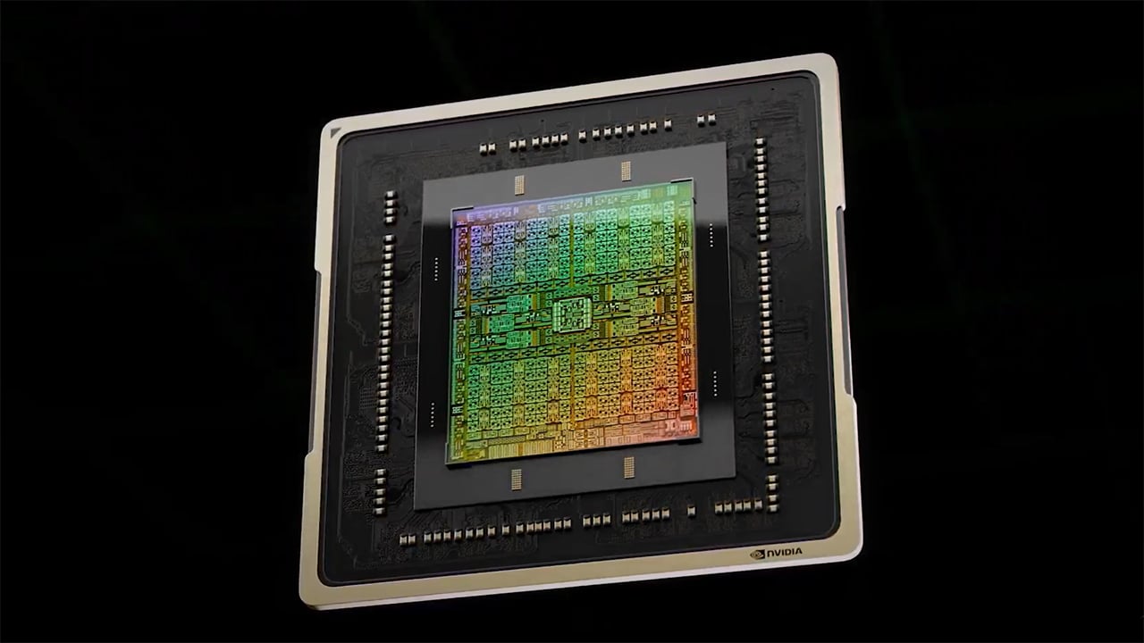
La GPU AD102 is the heart of the GeForce RTX 4090 and, as we have already learned in the past few hours, it is a chip from 76.3 billion transistors crammed into an area of 608.5 mm2. La GPU ha 144 Streaming Multiprocessor, 18432 CUDA core, 144 RT cores and 576 Tensor cores. Also on board 192 ROPs and well 96 MB of L2 cache. The memory interface is 192 bits.
The GeForce RTX 4090 does not implement the GPU in full form, however, as we were able to explain in a news in which we hypothesized the future arrival of a 4090 Ti. The RTX 4090 provides 16384 CUDA cores active as a result of 128 working SMs, 128 RT cores and 512 Tensor cores. The data of the ROPs is equal to 176 units, while the bus remains at 384 bits.
The GPU AD103 provides instead 45.9 billion transistors in an area of 378.6 mm2. The chip provides 80 Streaming Multi processors for a total of 10240 CUDA cores, 80 RT core and 320 Tensor core. The provides 112 ROPs and delivers 64MB L2 cache. The memory interface is 256 bits.
There is no fully active AD103 on board the GeForce RTX 4080 16 GBin fact the number of MS drops to 76 leading to the following specifications: 9728 CUDA core, 76 RT core and 304 Tensor core. The ROPs are present in a number equal to 112.
Finally, we come to AD104GPU that according to what we learn is integrated into the GeForce RTX 4080 12 GB in its full form. The chip has an area of 294.5 mm2 and integrates 35.8 billion transistors. On board there are 60 SM for 7680 CUDA core, 60 RT cores and 240 Tensor cores. The L2 cache is equal to 64 MB, while the ROPs are 80. The memory interface is 192 bit. We summarize in the following table the specifications of the Ada Lovelace GPUs, along with the GA102 for reference:
| AD102 | AD103 | AD104 | GA102 | |
| Architecture | There’s Lovelace | There’s Lovelace | There’s Lovelace | Ampere |
| Productive process | TSMC 4N | TSMC 4N | TSMC 4N | Samsung 8N |
| Transistor | 76.3 billion | 45.9 billion | 35.8 billion | 28.3 billion |
| Die size | 608,5 mm² | 378,6 mm² | 294,5 mm² | 628,4 mm² |
| Streaming Multiprocessor | 144 | 80 | 60 | 84 |
| CUDA Core | 18432 | 10240 | 7680 | 10752 |
| Tensor Core | 576 | 320 | 240 | 336 |
| RT Core | 144 | 80 | 60 | 84 |
| ROPs | 192 | 112 | 80 | 112 |
| Cache L2 | 96 MB | 64 MB | 48 MB | 6 MB |
| Bus | 384 bit | 256 bit | 192 bit | 384 bit |
Putting aside the number of cores, it is evident that NVIDIA has decided to follow AMD on expanding the cache inside the chips. AMD with RDNA 2 has implemented an Infinity Cache up to 128 MB, a memory that has allowed it to maintain a reduced memory interface but still guarantee a high overall bandwidth.
NVIDIA does the same thing with Ada Lovelace, albeit in a different way, with up to 96MB of L2 cache that stands out from the 6MB L2 cache found in the top-of-the-line GA102 RTX 3000 series GPU. L2 cache NVIDIA has decided to sacrifice the NVLink interconnect.
Finally, it is good to remember that all these GPUs are manufactured at TSMC with a process called 4N which is not to be confused with TSMC’s own N4. 4N is to be seen as a ‘optimization for NVIDIA of the Taiwanese company’s N5 (5 nm) process.
Related posts:
 7-nanometer Nvidia GPU, TSMC will handle most of the production
  ASRock X299, a new BIOS allows you to install 2 TB of memory
  MSI Prestige X570 Creation Review: Test | Specs | Hashrate
  Radeon RX 5500 XT, PCI Express 3.0 castrates performance?
  An overclocker ran 1TB of RAM on an X299 motherboard limited to 256GB
  Best Review 2021: MSI MPG X570 Gaming Edge WiFi Under $250 ($200)