Later this year, graphics circuit makers will begin the transition to 14 nanometers, more than four years after the introduction of 28 nanometers. This leads to doubled transistor density and thereby the possibility of more advanced circuits with higher energy efficiency. The technology can be expected to bring great benefits regardless of performance segment.
Now a former AMD employee at Linkedin is revealing a previously unknown graphics circuit that goes by the alias “Project F”. The description states that it will be manufactured on 14LPP, the card for 14 nanometers Low-Power Plus, at Globalfoundries and Samsung, which have a collaboration around the technology.
Furthermore, it also appears that the circuit measures in at 232 mm2, which is close to the 212 mm2 which applies to Pitcairn, later known as Curacao and most recently Trinidad in the Radeon R9 370 and R9 370X. Thus, it is likely that Project F is a circuit intended for the middle class rather than the upper performance segment.
Provided that AMD succeeds in capturing the improvements in the new manufacturing technology, it is possible that the graphics circuit performs similarly to Hawaii, which is used in the Radeon R9 290, R9 290X, R9 390, R9 390X and measures in at 438 mm2. This at the same time as power consumption has the potential to be halved.
The launch of the Polaris architecture with associated graphics chips, of which Project F is believed to be one, is scheduled for mid-2016.
Source: Videocardz.
Related posts:
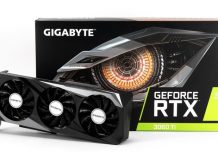 Review & Test: Video card Gigabyte GeForce RTX 3060 Ti Gaming OC Pro
 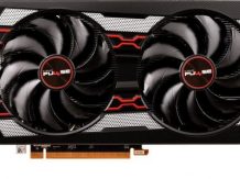 AMD Radeon RX 5600 XT VS GTX 1660 Ti and RTX 2060: Review| Set-up| Hashrate
 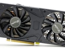 Review of the KFA2 GeForce RTX 3060 Ti Core video card
 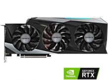 GIGABYTE GeForce RTX 3090 Gaming OC video card: Review| Specs | Set-up|
 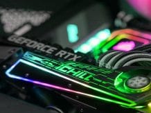 INNO3D GeForce RTX 3090 iCHILL X4 video card review: Test | Config | Hashrate
 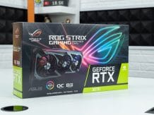 ROG Strix GeForce RTX 3070 OC Review: Test | Specs | Hashrate