– Following the Computex announcement of 15 percent more IPC, AMD today revealed all the technical details about the new Zen 2 architecture. Almost every detail has been changed; in the end, Ryzen 3000 is an all-round faster package that emerges with up to 16 cores to become the most powerful desktop processor.
AMD is launching Zen 2 26 months after the start of the first Zen processor generation. Many of the original ideas continue, but no fewer things have been changed. This begins with the visible part of the processors, as long as there is no heat spreader, such as the outsourcing of many elementary functions of a CPU to a special, separate I / O die, and continues to the transistor level. Combined with an optimized infinity fabric, previous vulnerabilities were addressed, from now on Zen 2 should be able to address much faster memory, for example. This is garnished with the first-time use of PCI Express 4.0, which should upgrade the entire platform.
Zen 2 should be smaller, stronger, more scalable and compatible
AMD's design guidelines for its own CPU department for the development of Zen 2 were clear: not only should the performance be increased in the desktop, but the scalability on the well-known AM4 socket should also be retained. The result is more cores, but also improved I / O, and all on the same AM4 platform, so that older motherboards can be retained with a CPU upgrade.
The leap in the production of 14 nm and 12 nm with Zen and Zen + to the new 7 nm production should significantly increase efficiency. TSMC ensures implementation with AMD's specifications and delivers impressive numbers: A CPU complex (CCX) consisting of four cores and 16 MB L3 cache is 47 percent smaller in 2019 than its predecessor: 31.3 mm² to 60 mm² ,
A CPU die emerges from two CCXs and is large for eight cores, 32 MB L3 cache and parts of the 74 mm² interconnect infinity fabric. A Ryzen 7 3700X as the direct successor to the Ryzen 7 2700X is 75 percent more efficient with the same number of cores and threads – a huge leap.
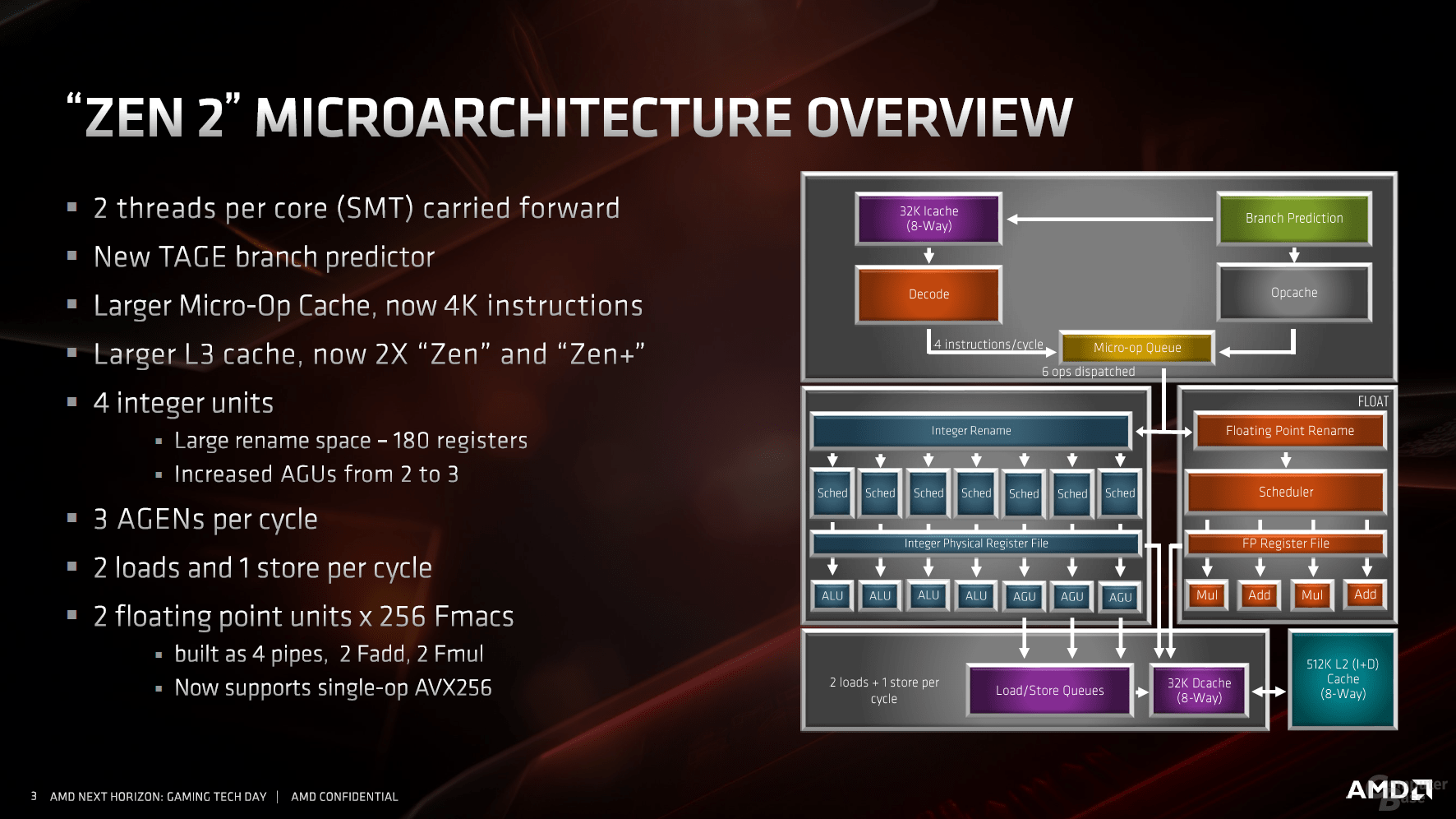
Overview of Zen 2
image 1 from 2
It all starts with the core
After the turnaround from module architecture back to classic CPU design, AMD continues on this path. The basic configuration is identical: One core should continue to provide two threads, the so-called SMT support.
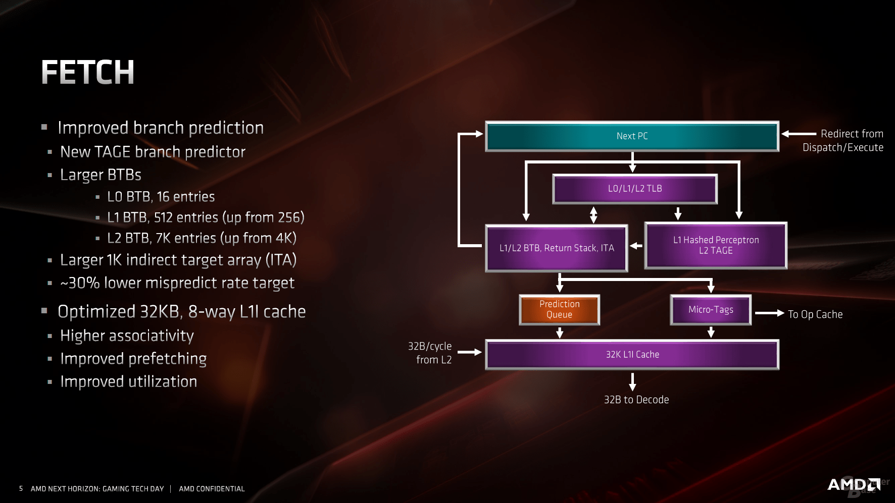
Doubled L0 cache and improved jump prediction
As with any CPU manufacturer, the first point of contact for performance improvements is the jump prediction. With all modern processors from Intel and AMD, this is supported by a micro-op cache, which holds data that it already knows. This means that the entire pipeline does not have to be seized, instead it can be shortened and the data transferred directly for execution. AMD has also recognized the great value of this quasi-L0 cache introduced with Zen for the first time at AMD, it is now twice as large as its predecessor and comprises 4,096 entries.
Fetch in Zen 2
image 1 from 2
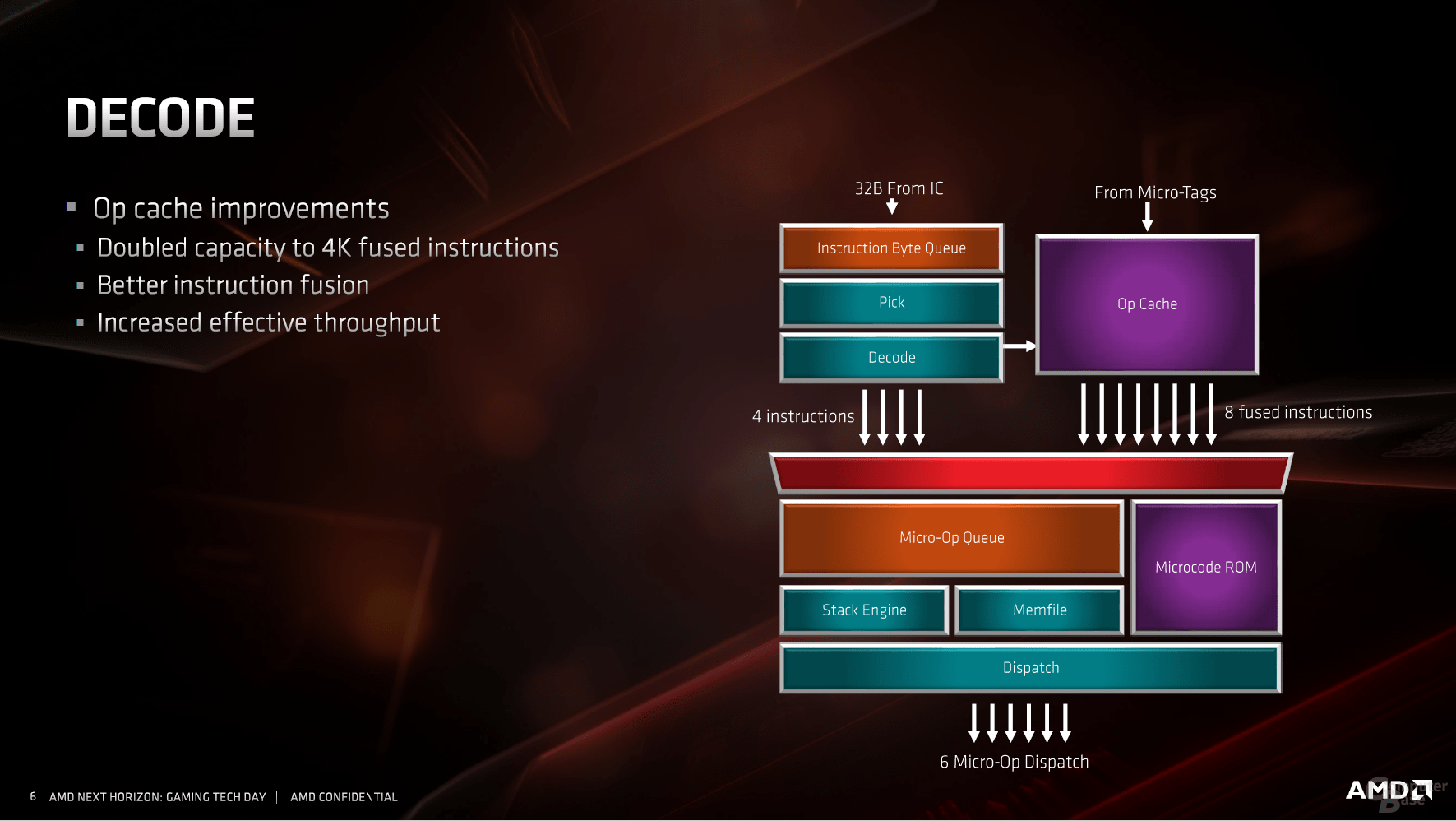
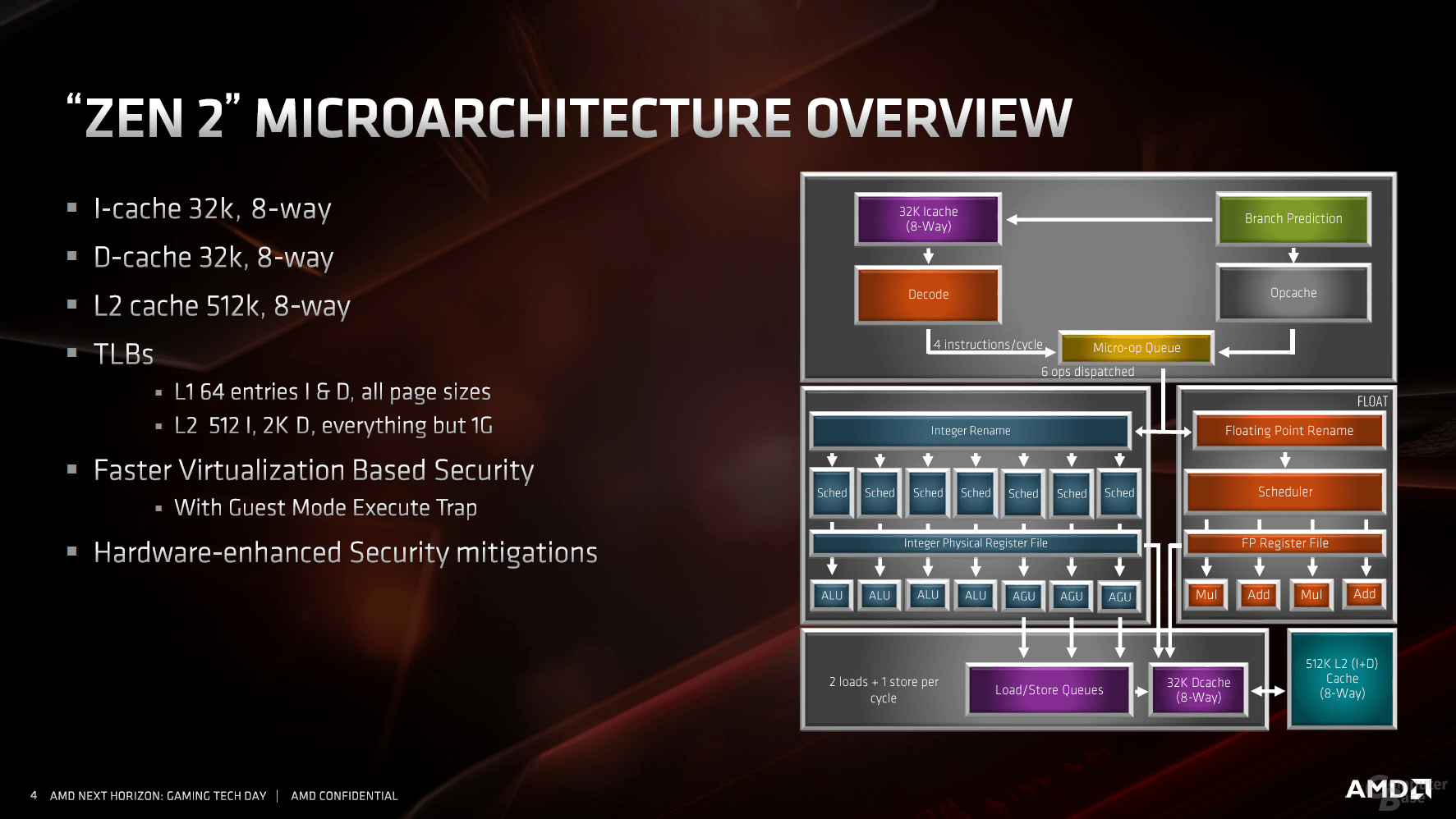
If the inquiries go the traditional way, the new jump prediction helps, for which many small parameters have been changed and largely drilled out. The most striking point is the L1 instruction cache, which has been halved from 64 KB to 32 KB. With a fourfold to eightfold increased associativity and further adjustments, the L1 instruction cache should nevertheless work more effectively. Like the previous generation, each Zen core ultimately decodes four instructions per clock cycle and, together with the micro-op cache, feeds the two schedulers for integer and floating point calculations.
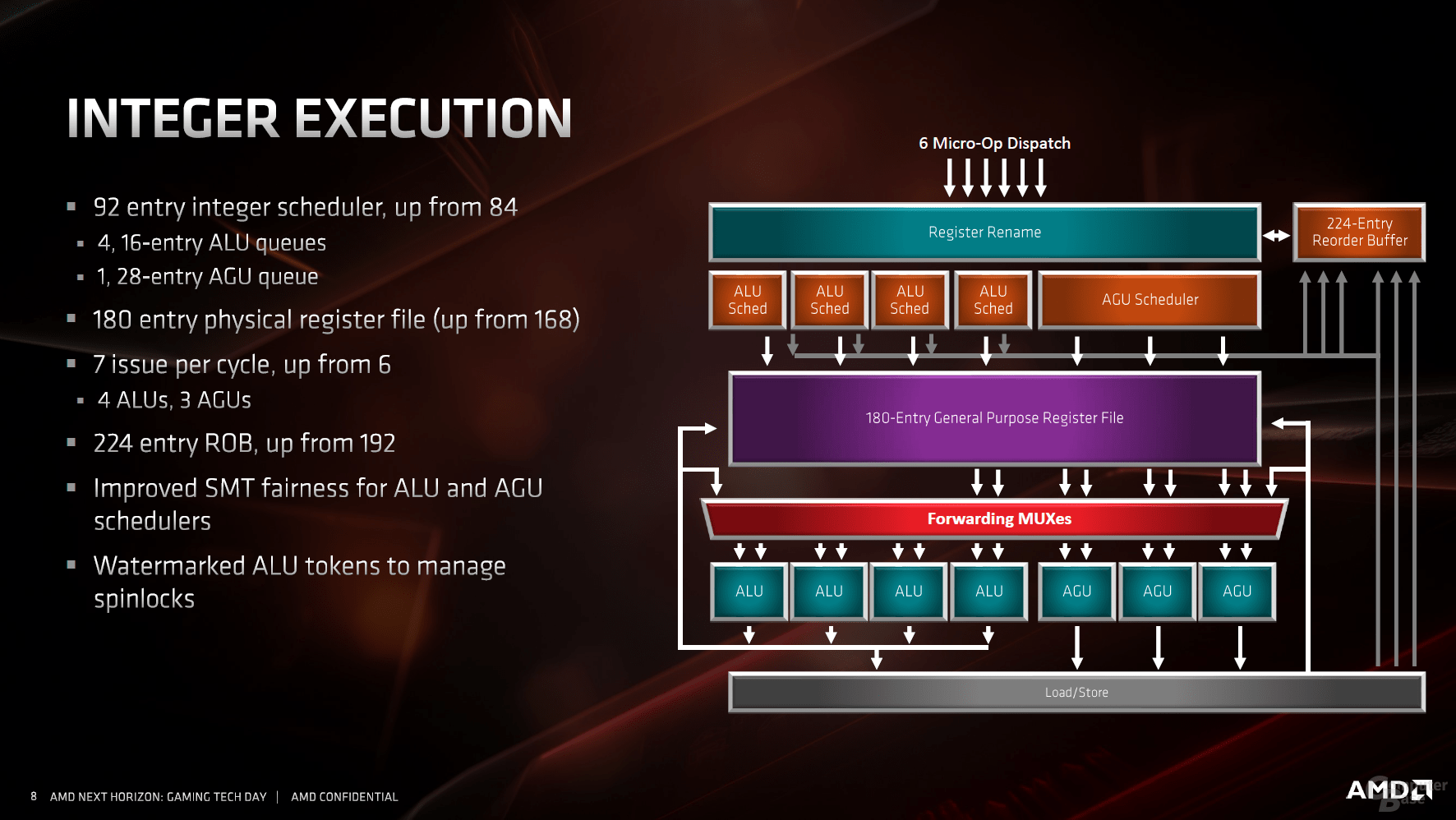
Integer and floating point execution units removed
The most striking changes in the area of the executing units can be found on the integer page. As in all other areas, the buffers were also expanded there, an additional AGU (address generation unit) for memory commands marks the difference to Zen.
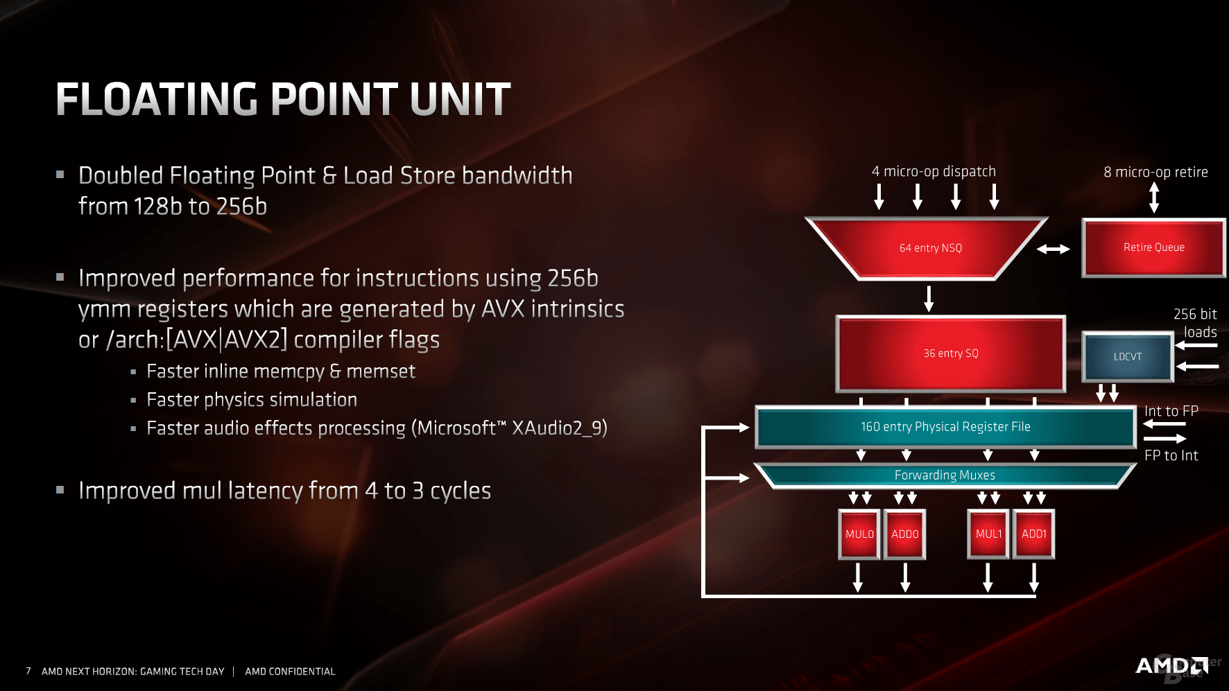
As a major innovation, the floating point range now offers twice the bandwidth, which benefits the modern AVX2 instructions. With the previous architecture, two 128-bit lines had to be interconnected to form an AVX-256, now the job is done by a pipeline alone. This effectively doubles the performance.
Load / store units and the cache follow the scheme
The load and store units follow the general trend towards optimization and enlargement. The TLBs hold more data and the latency has been reduced. This is followed by the 32 KB L1 data cache, which should benefit from the doubled bandwidth.
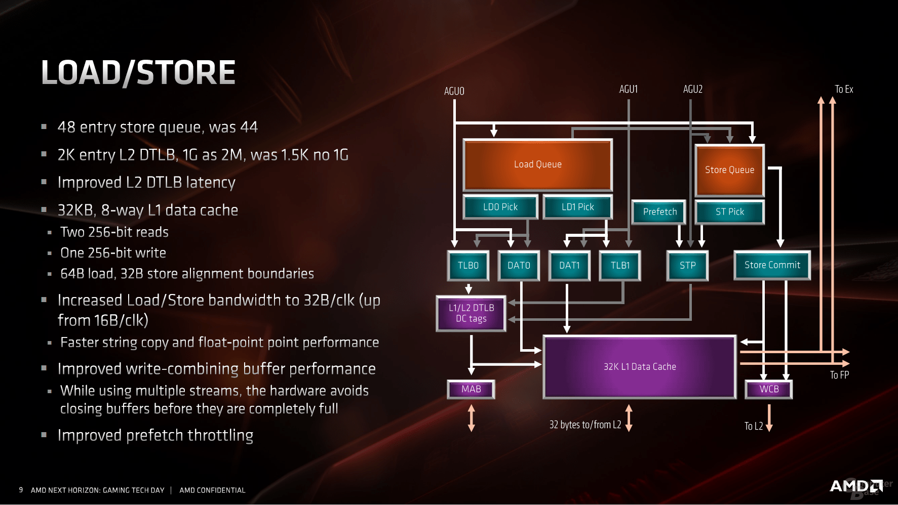
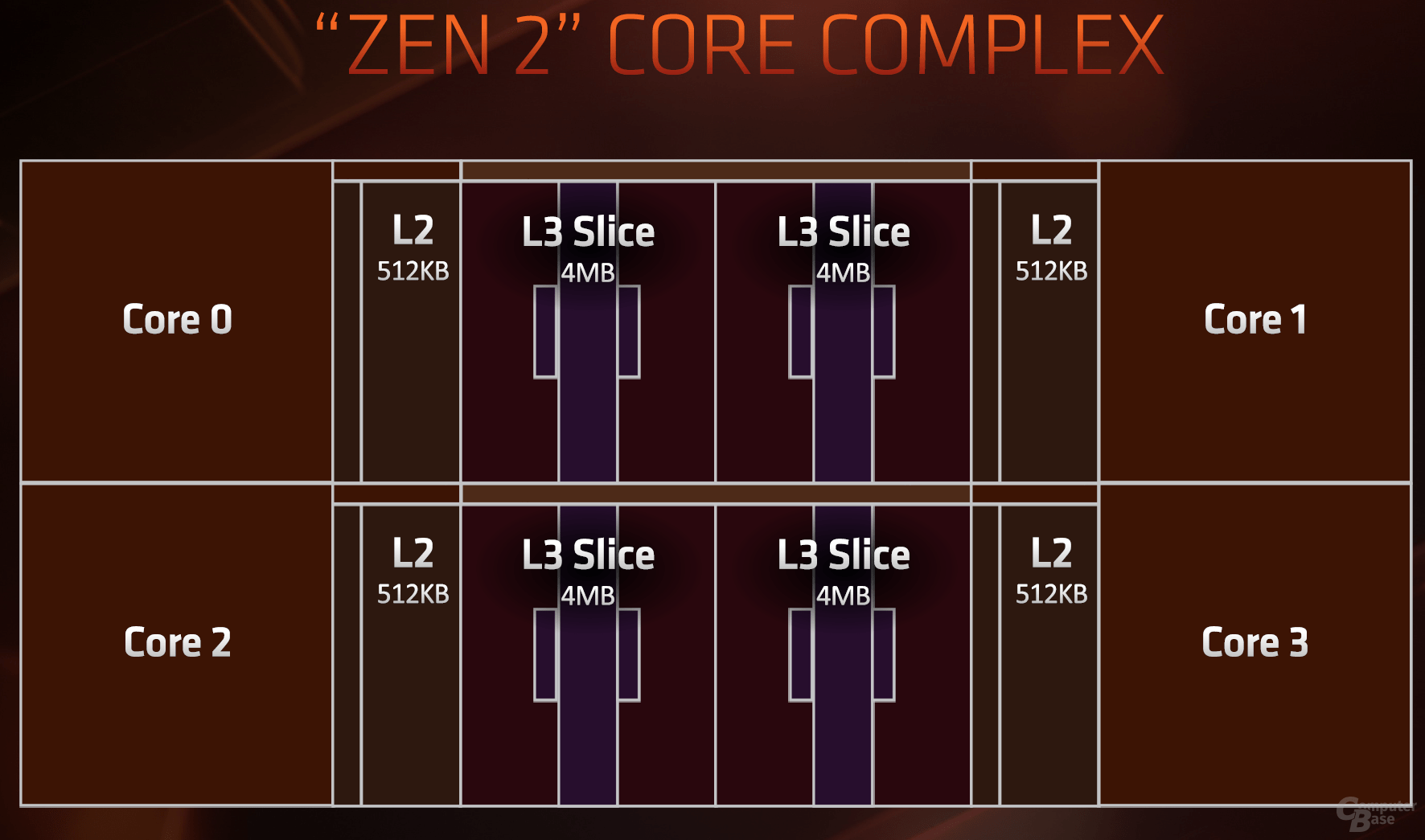
The caches are and remain a core theme of Zen 2, which should support the interaction of all subareas as diverse and as quickly as possible. The L1 cache is traditionally followed by an L2 cache, which is still 512 KB per CPU core. There is a shared 16 MB L3 cache per CCX, i.e. for four cores. But this is divided into four slices, each with four megabytes – this already looked like this with Zen.
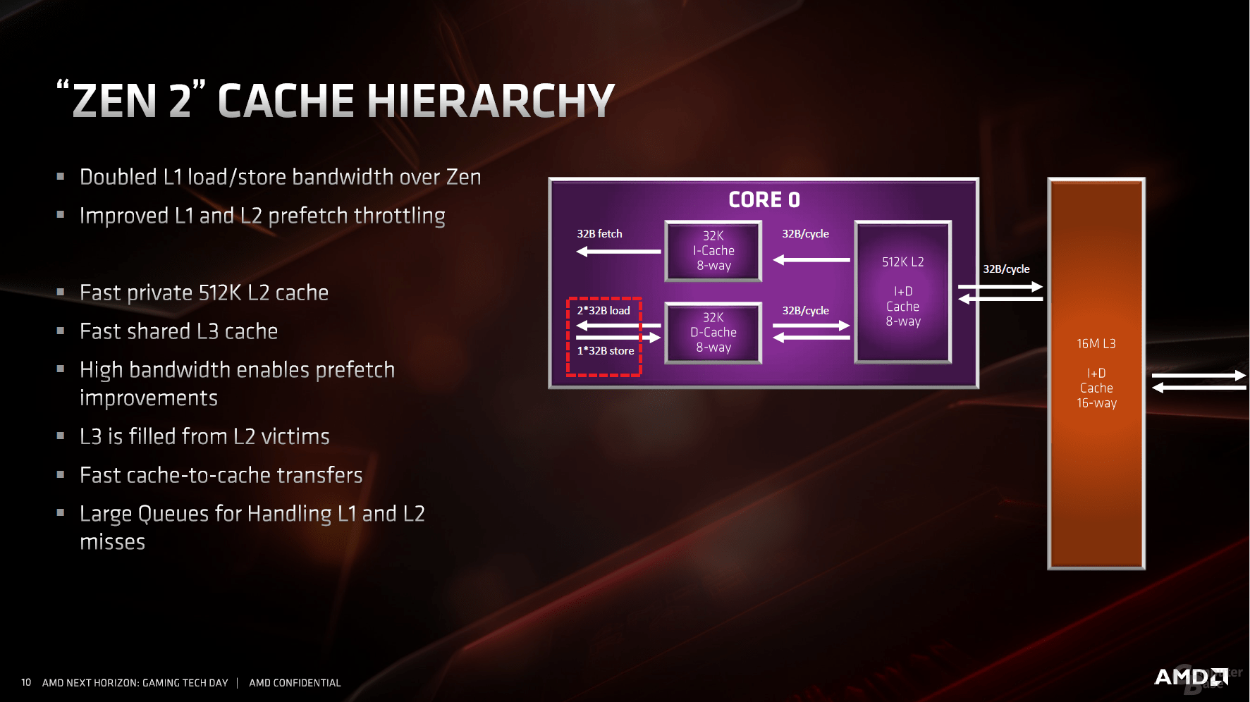
Cache hierarchy in Zen 2
image 1 from 2
Two CCXs become one CCD
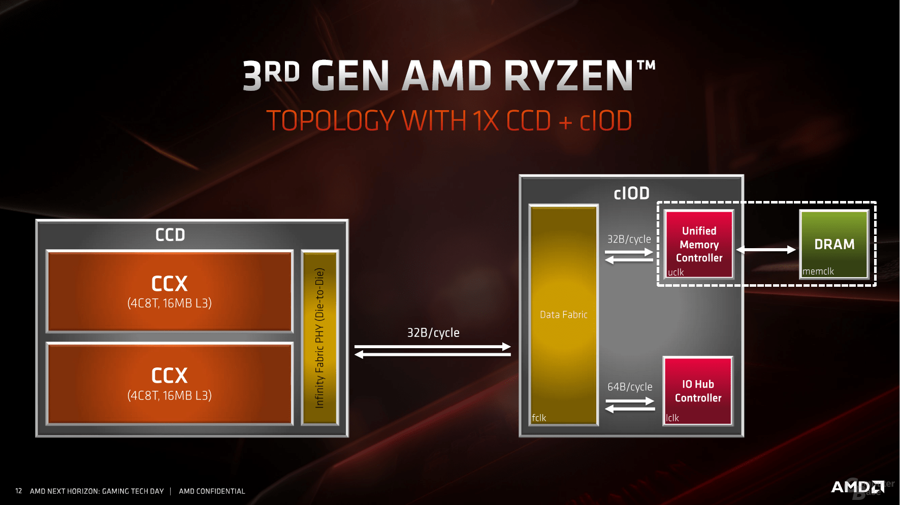
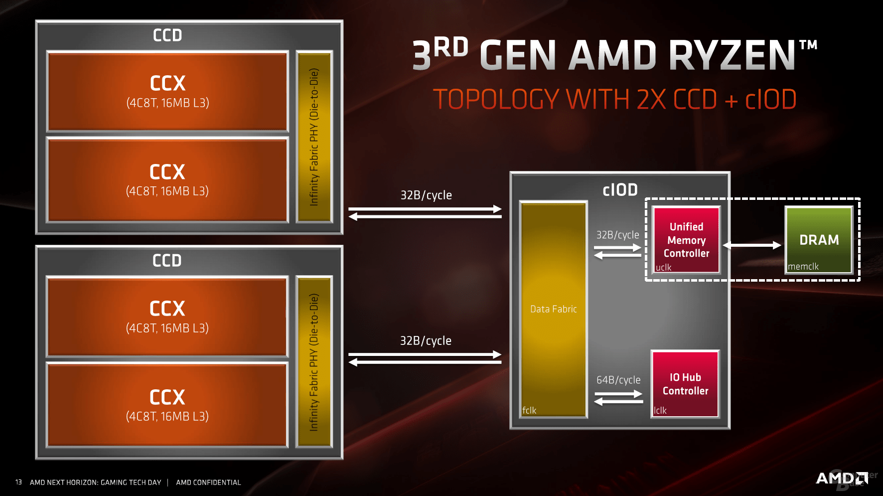
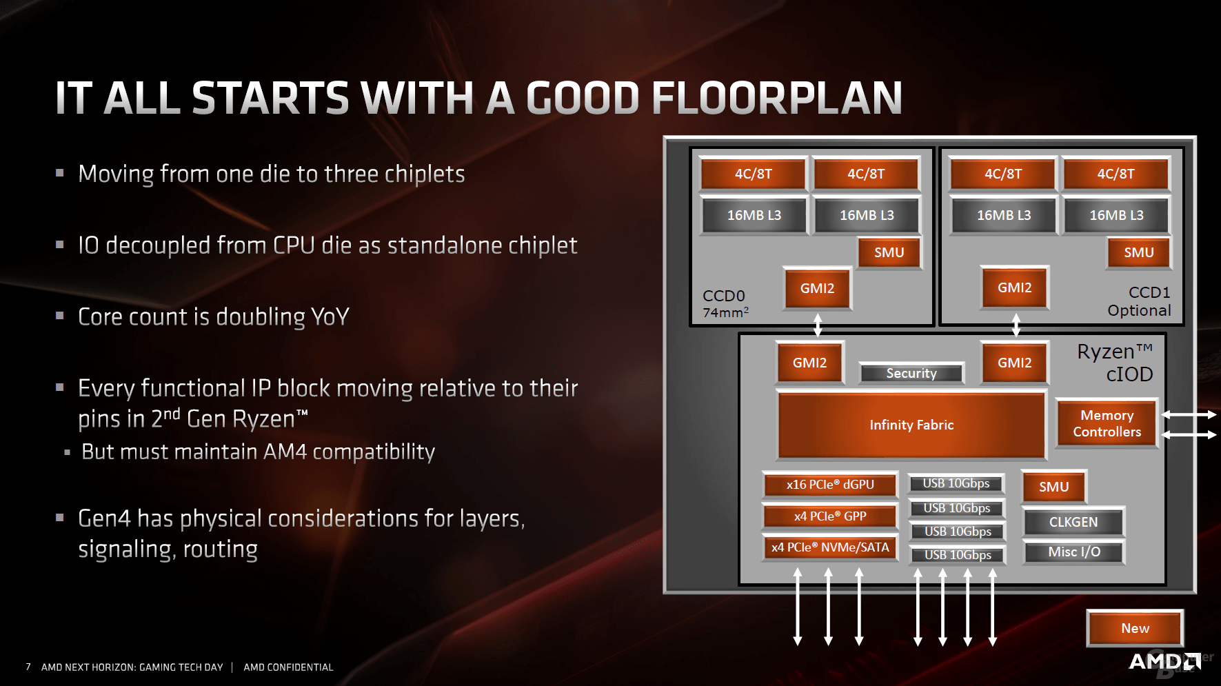
The CCX procedure from the previous generation Zen will continue as before. However, the memory controller and I / O features such as the PCIe lanes are now missing, instead they are represented in the new I / O die. Depending on the model from the Ryzen 3000 family, a so-called CCD consisting of two CCXs is used, or two – for 8 cores or 16 cores of the CPU.
Zen 2 CCX
image 1 from 4
The multi-chip approach is impressively continued on socket AM4
Zen brought the multi-chip design back onto the big stage. In the past, this approach was normal, all of Intel's first quad-core processors were multi-chip CPUs based on two dies. At that time AMD brought the native design and teased against Intel, two years ago Intel's return carriage came against AMD and the competitor spoke of "glued this together". But it doesn't work without multi-chip solutions, Intel also knows that and has recently been offering such CPUs again. And AMD's confirmed approach goes to the next level with Zen 2 at Ryzen 3000.
Multiple chips on a package provide a cost advantage. Because producing smaller chips is easier, the yield per wafer is higher because the space is better used. Both contribute to the fact that Ryzen 3000 does not ultimately become more expensive despite the use of the expensive 7 nm production from TSMC. The CPU dies are combined with the I / O die, in which the production stage is not equally important. That is why AMD uses the significantly cheaper 12 nm process from Globalfoundries.
New infinity fabric is significantly faster and more efficient
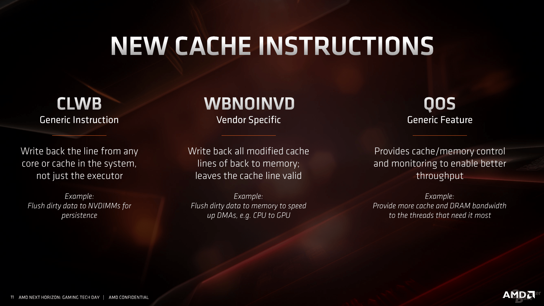
The multiple chip approach depends on the connection. The second generation Infinity Fabric not only deals with the modular structure even better, first of all the bandwidth was increased so that PCIe Express 4.0 could be realized. At the same time, the connection was worked on in the sense that it both transfers data from one cache to another more quickly and also enables queries to the RAM with lower latency. In particular, the different latencies were sometimes a problem with the first generation, but this was primarily present in the server area. It will have to be shown how well the new Infinity Fabric handles eight CPU dies and one I / O die.
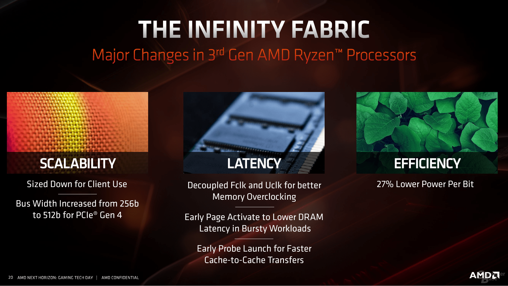
For the desktop page, other things are in the foreground. The clock CPU (fclk) and memory controller (uclk) were decoupled, but are still coupled to a certain extent to the infinity fabric, which ultimately has a positive effect on the behavior of (overclocked) DDR4 memory. From DDR4-3733 the divider changes internally from 1: 1 to 2: 1, with a slight disadvantage for the latency.
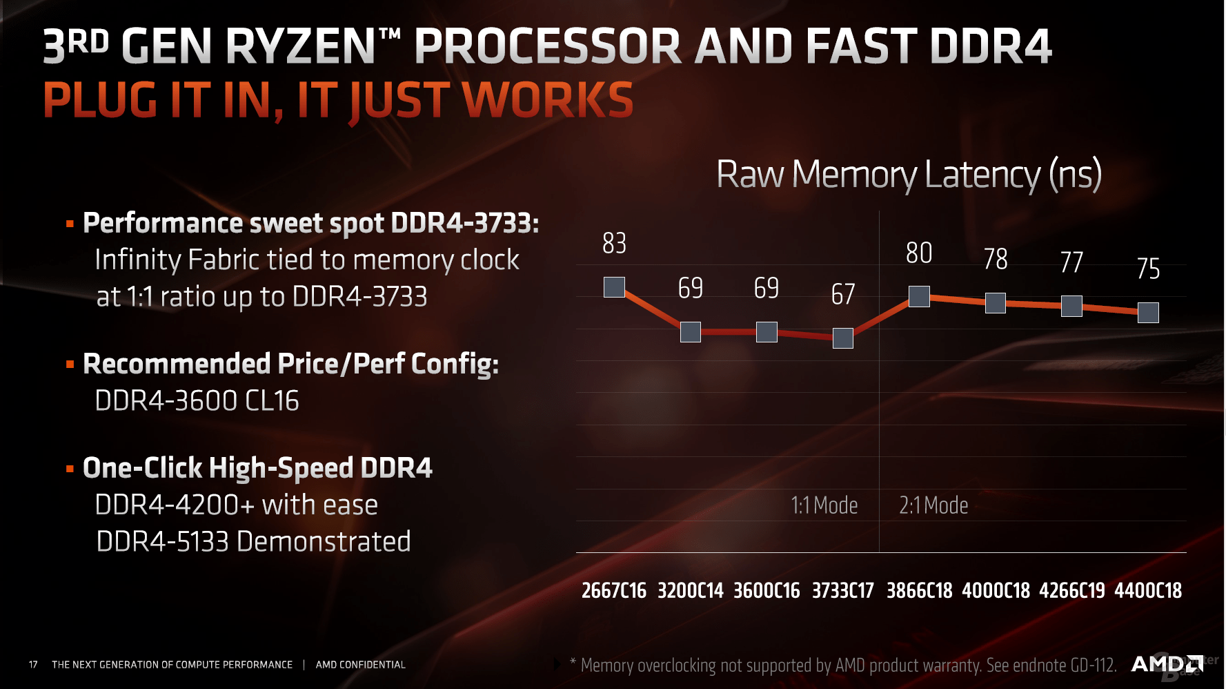
From then on, a maximum of only DDR4-3800, for example, is no longer possible; AMD has already demonstrated values beyond DDR4-5100 with the new processors. DDR4-3200 is used natively, AMD recommends DDR4-3600 as the best solution in terms of price / performance. In view of the low and falling prices for DDR4 memory from BitcoinMinersHashrate, there is nothing wrong with this recommendation.
The "old" socket AM4 specifies the rules for the package
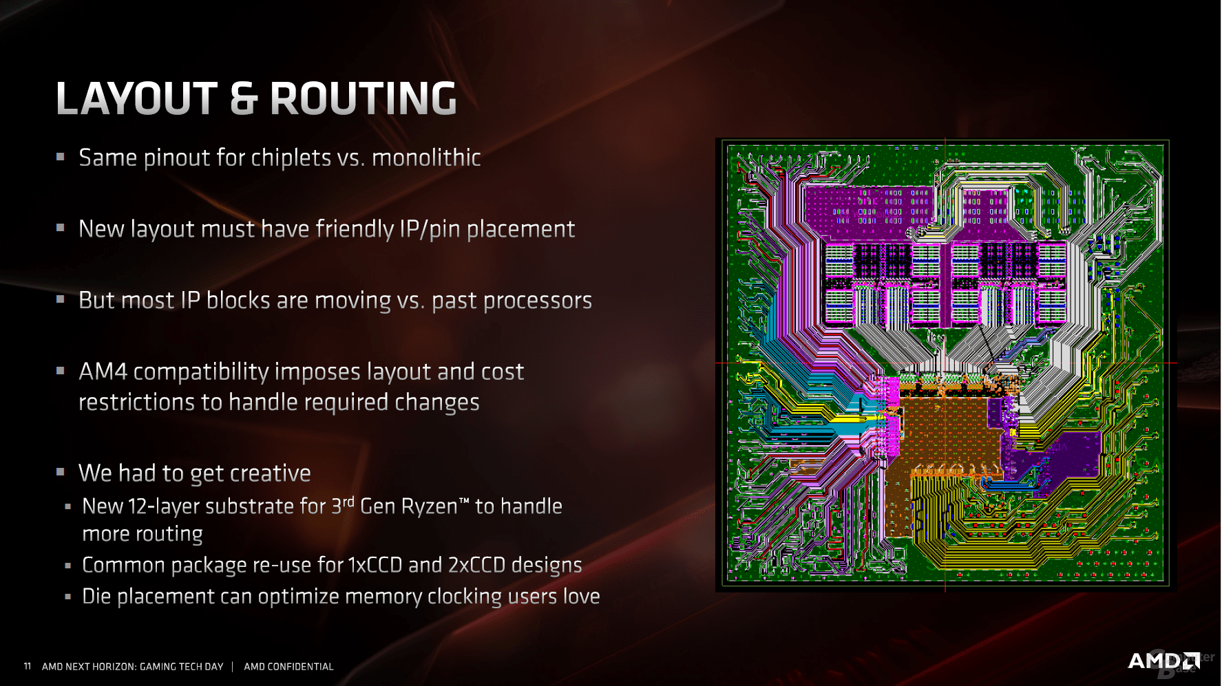
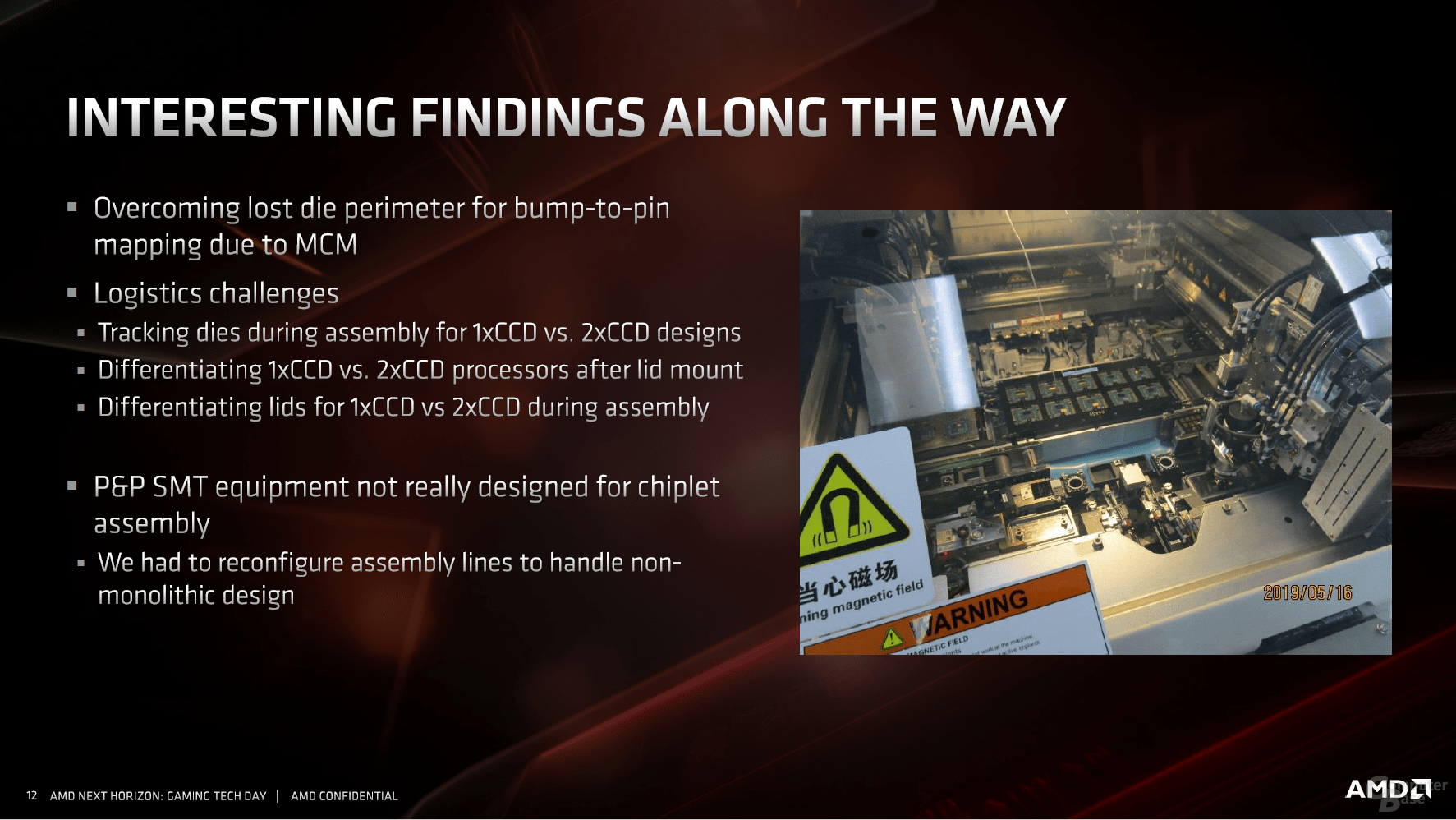
According to AMD, a challenge was the continuation of the completely new design on the previous base. The up to three dies require a 12-layer package to bring the signals neatly to their respective destinations. This is not only due to PCIe 4.0, almost every section of the overall product is located differently from Ryzen 2000, but the data supplied must nevertheless be routed to the appropriate pins.
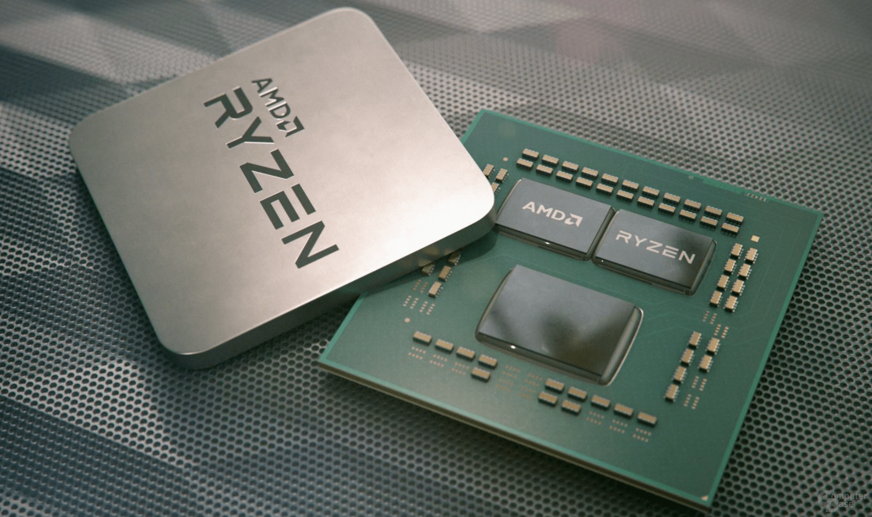
Package with several chips
image 1 Of 3
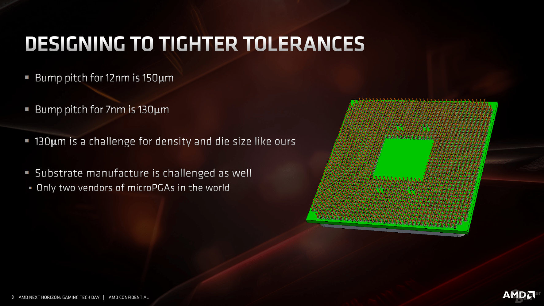
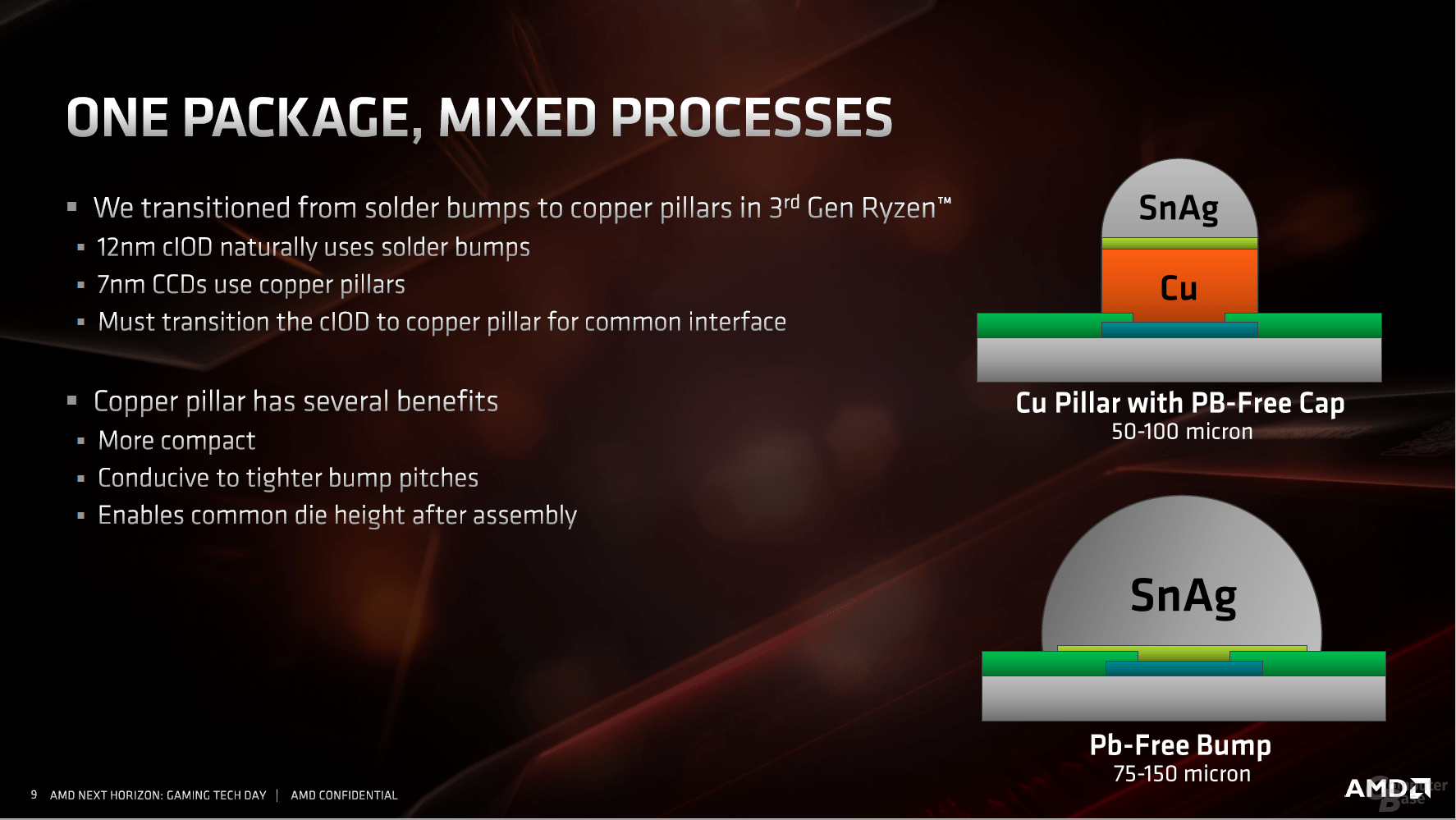
In addition, there is a mix of two different technology levels in one package, for which different materials are used. The chips no longer rely on classic soldered BGA contacts as up to Ryzen 2000, but on so-called copper pillars. These are significantly smaller and promise a higher current carrying capacity with lower electrical resistance, lower inductance and better resistance to electromigration. The process has been proven in the CPU area for 15 years, Intel has been using it since Presler, Yonah & Co.
Finally, all changes have to be included on the package. Since there are small processors that only use one CPU die in addition to the I / O die, but others use two, the production process had to include these steps. Overall, just this alignment in the production lines required a lot of logistical work, explained AMD. In the end, three large companies and countries are responsible for this, which are also immortalized on the heat spreader of the CPU: Globalfoundries from the USA for the I / O chip, TSMC from Taiwan for the CPU dies and AMD's packaging plants in China : "Diffused in USA, Diffused in Taiwan, Made in China".
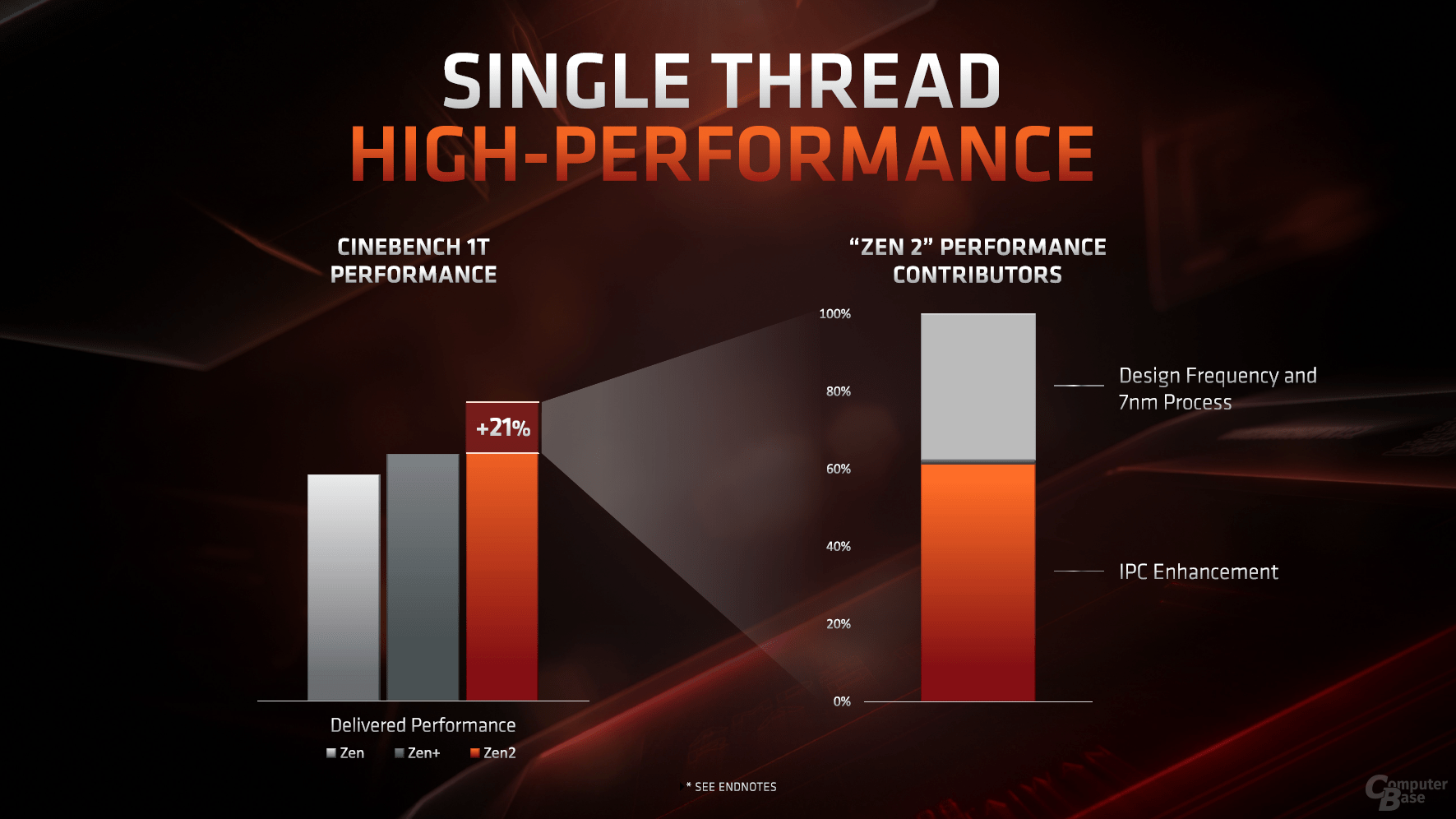
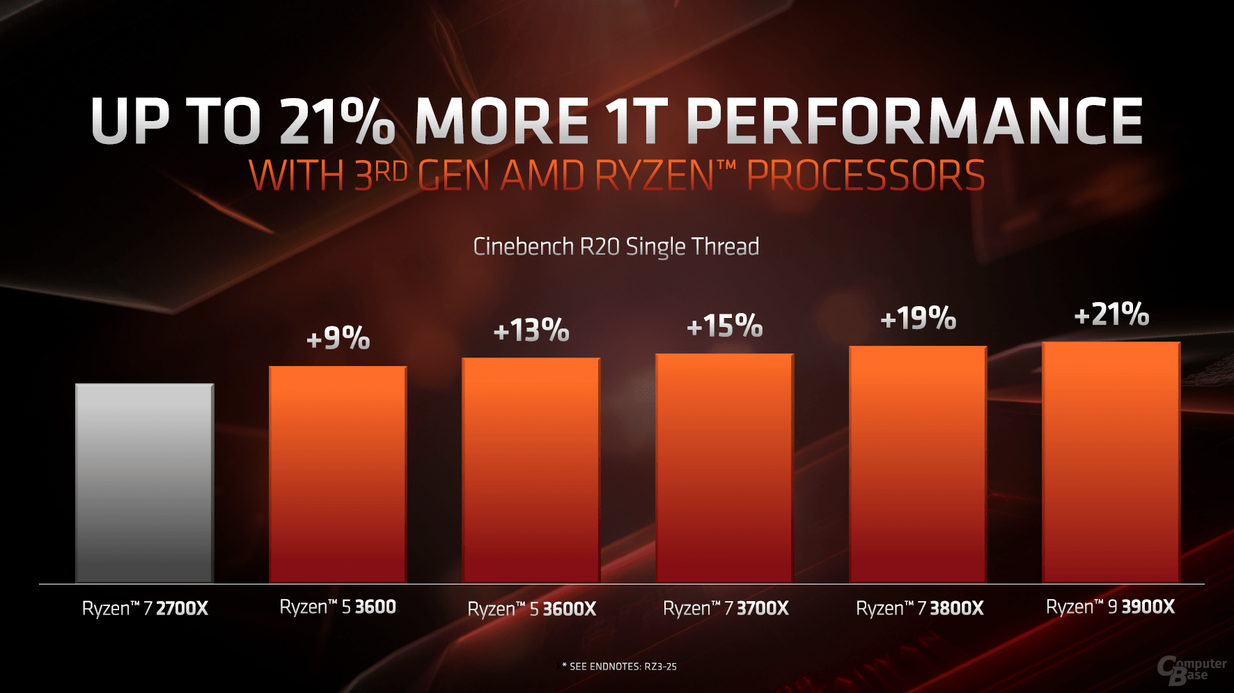
Multi-threaded an emperor, now single-threaded too?
Since the start of the first Zen generation, despite the big leap to the predecessor bulldozer, the lag in performance in applications for only one core has been criticized. However, the mixture of a new production stage, higher cycle times and further improved IPC make for Ryzen 3000 a huge set in the single thread performance class. According to the AMD, the plus is up to 21 percent compared to Zen +, i.e. the Ryzen 2000.
Single-threaded performance
image 1 from 2
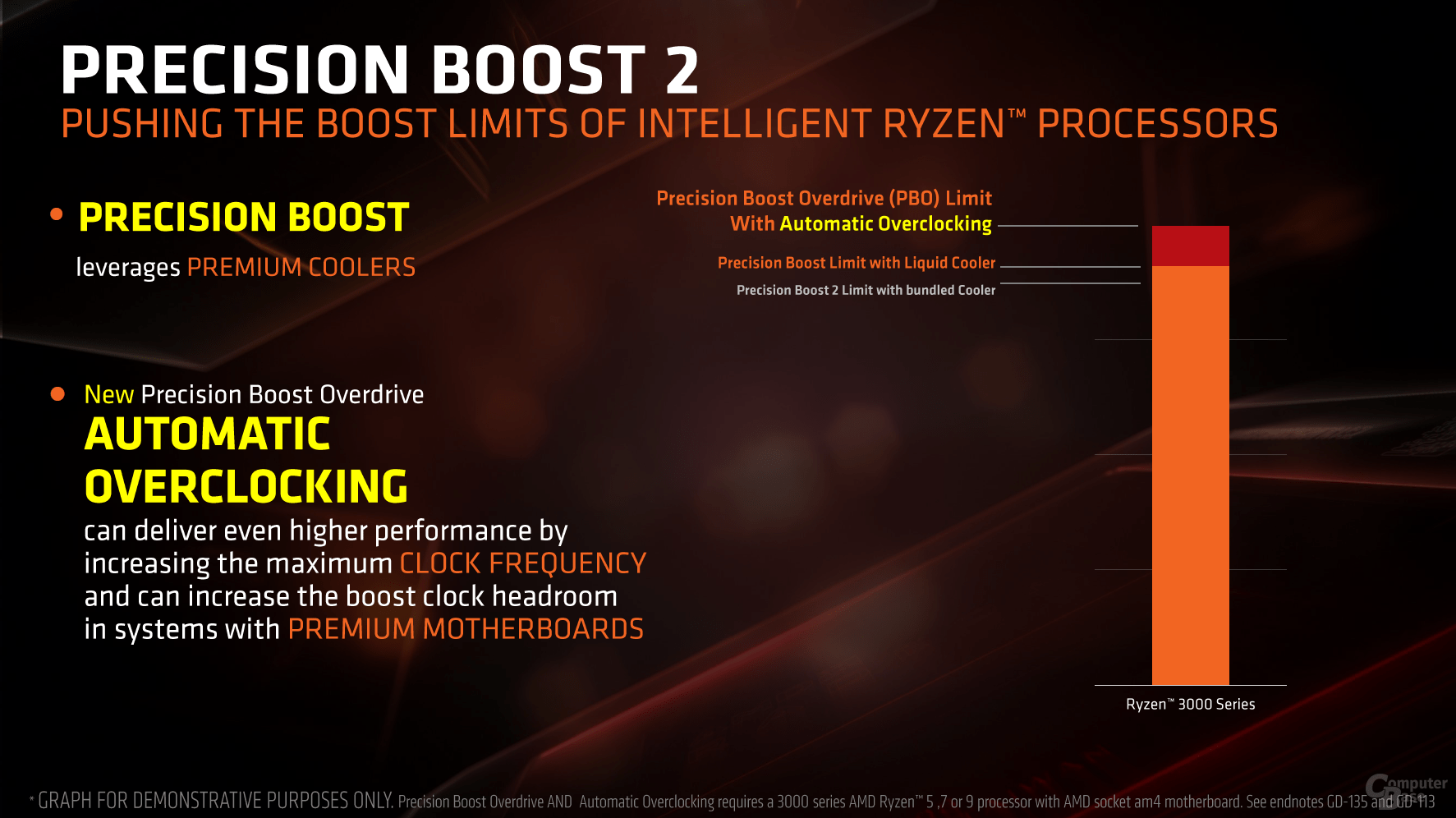
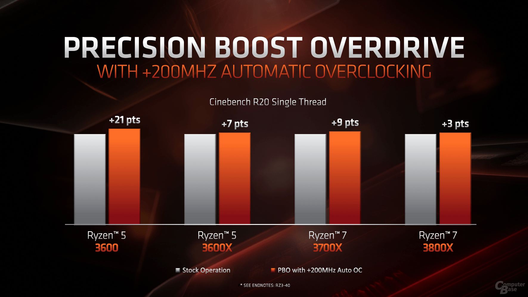
The multi-thread performance determines the number of cores and the clock, in addition there is SMT. SMT should behave similarly to what it was before, maybe even a little better, explains AMD, because there were also some optimizations there. With regard to the clock, the bonuses of Precision Boost 2 and Precision Boost Overdrive also apply. With good cooling, an automatic overclocking of up to 200 MHz is also possible. XFR, as it used to be, no longer exists. All of this now runs within the normal turbo.
Precision Boost 2 and PBO
image 1 from 2
The Ryzen 3000 model range at the start
AMD will market six processors as a Matisse processor family, five will be available from July 7, and thus on the same day as the Radeon RX 5700 XT and Radeon RX 5700, the flagship Ryzen 9 3950X with 16 cores will follow in September , This CPU competes in die yield with the Epyc-2 server processors, which rely on eight-core dies to provide 64 cores. Such a spin-off is expected as a Threadripper 3000 in the high-end area, but not before the end of the year or not until 2020.
As introduced last, there will no longer be pure Ryzen 3 CPUs, this is the task of the APUs, the CPUs only start with the Ryzen 5. In line with this, AMD has officially launched two new solutions with its two Picasso desktop processors.
Optimizations with Windows 10 May 2019
AMD's CPU architectures and Windows 10 were often at war at the start. Everything works, but not as well as with later patches. This was already the case with Bulldozer & Co., even Zen didn't show its full potential for the launch. The current May 2019 update of Windows 10 brings some improvements and optimizations for the Ryzen 3000 family. Among other things, this means that the cores are used in one CCX before jumping to another. This significantly reduces latency, in the best-case scenario when games rely on a few cores, but these were previously distributed unevenly across the CCX, AMD calls 15 percent performance gain.
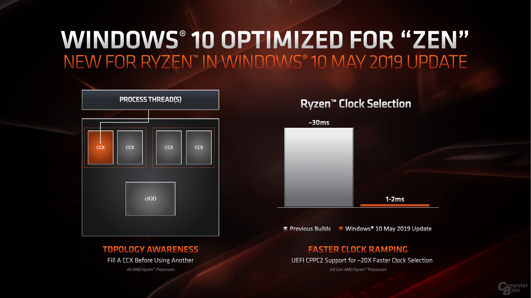
Windows 10 May 2019
image 1 from 2
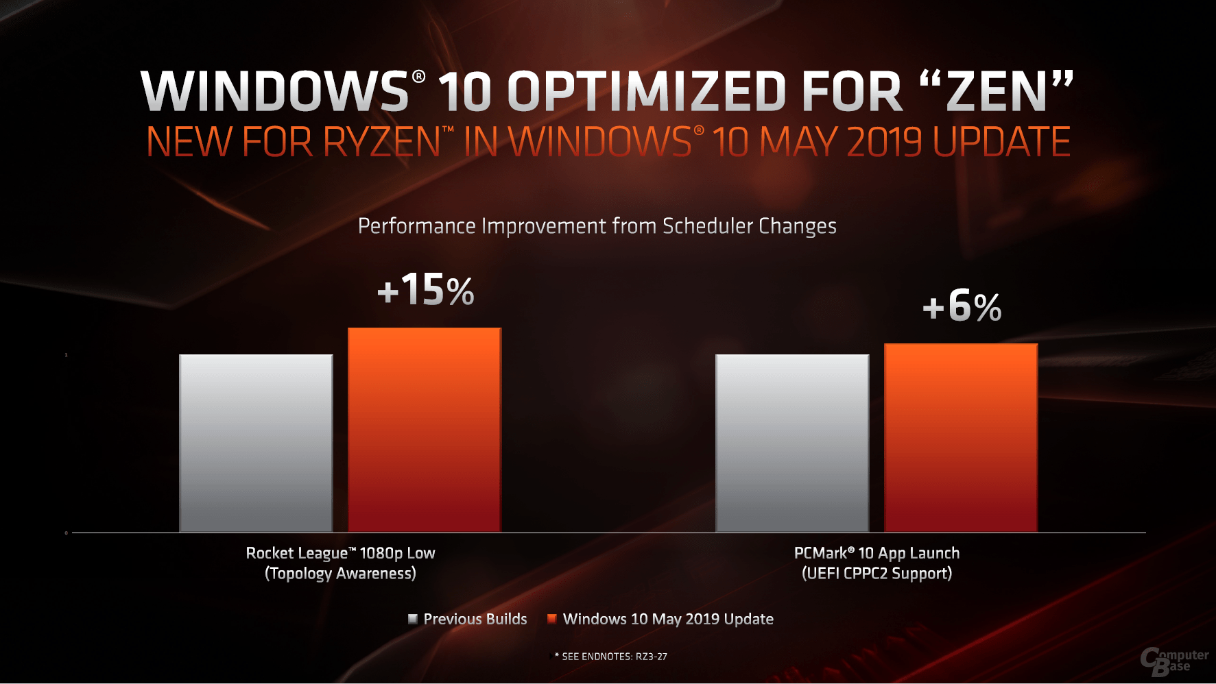
The Collaborative Processor Performance Control (CPPC2) on the other hand automatically ensures the right performance based on the requirements, but also based on the thermal conditions, which are provided by information from the operating system. The new Windows 10 update together with the new hardware and full CPPC2 support, for example in PCMark 10, ensures a small speed boost when starting applications.
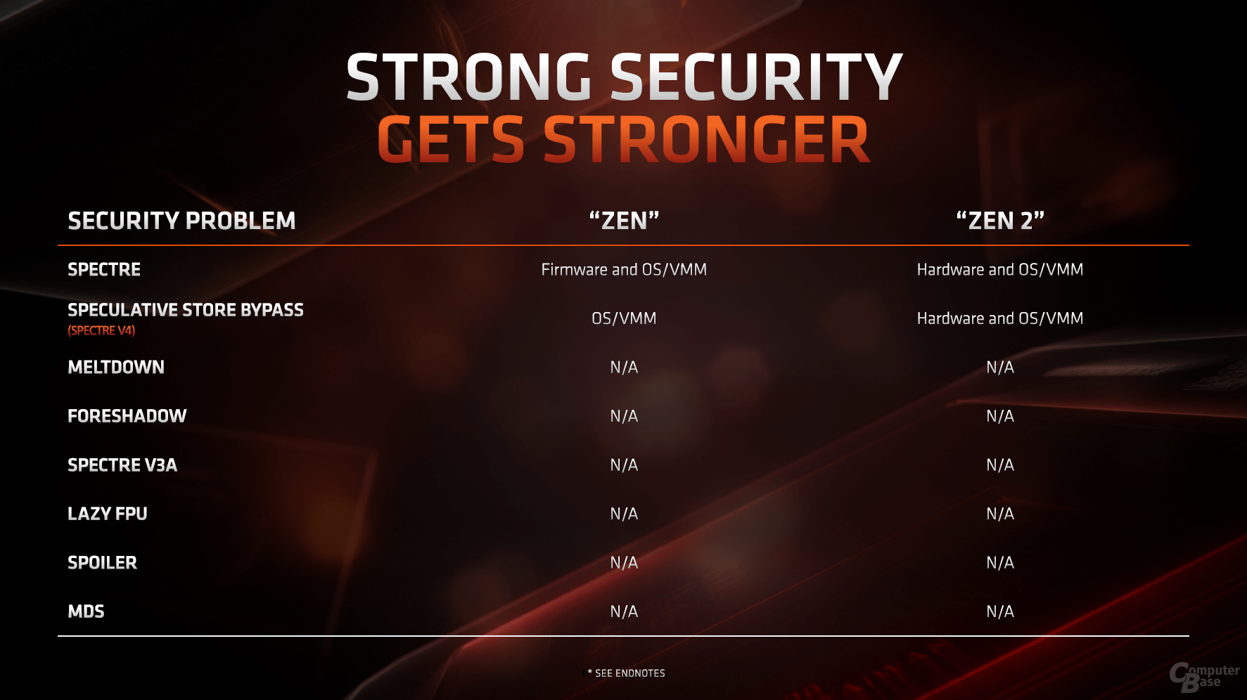
Zen 2 is (almost) completely secure
The huge security gaps in modern processors have partially shaken faith in industry. Almost all manufacturers are targeted, but not all are affected equally. In contrast to Intel, which was vulnerable to almost every vulnerability, AMD was only affected in some areas. The two Specter variants are now partly suppressed by the hardware, but even with Zen 2 it doesn't work without the operating system. AMD's architecture is currently immune to all other problems.
First impression
Extremely solid CPU craftsmanship meets very good manufacturing, and what has come out of it knows how to please at first glance. Almost all of the few weaknesses of the first generation were eliminated on paper, and the strengths also expanded. The IPC increase of 15 percent compared to Zen + is impressive. Within two years, the bar has been raised to just under 20 percent. After Zen already achieved more than 50 percent compared to bulldozers, there have rarely been in the past 30 years.
In addition, the performance is no longer very high only in multi-core load scenarios, but also in single-thread and especially in gaming, where Intel was the top dog. This caused the blue giant to take an early counterattack, the Core i9-9900KS with 5 GHz across all cores and threads – but this will only come in the fourth quarter.
The immediate availability of Ryzen 3000 means that nothing stands in the way of an independent assessment of the processors in the next three weeks. AMD not only provides the new X570 platform, two-year-old mainboards are also said to work. However, there is still a small question mark, until today there are hardly any executable BIOS available, many manufacturers speak of mid-June at the earliest – BitcoinMinersHashrate had to learn this first-hand. However, the majority of customers should consider a complete new purchase anyway in order to be able to use all features such as PCIe 4.0.
BitcoinMinersHashrate has received information about this report from AMD at NDA. The only stipulation was the date of publication, which was set by AMD. The provision of these materials was preceded by participation in a press event in mid-June in Los Angeles, USA. The costs of arrival and departure and accommodation were borne by AMD.
This article was interesting, helpful, or both? The editors appreciate any support in the form of deactivated ad blockers or a subscription to BitcoinMinersHashrate. More on the topic of ads on BitcoinMinersHashrate.
Related posts:
 7-nanometer Nvidia GPU, TSMC will handle most of the production
  ASRock X299, a new BIOS allows you to install 2 TB of memory
  MSI Prestige X570 Creation Review: Test | Specs | Hashrate
  Radeon RX 5500 XT, PCI Express 3.0 castrates performance?
 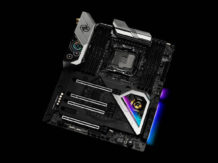 An overclocker ran 1TB of RAM on an X299 motherboard limited to 256GB
  Best Review 2021: MSI MPG X570 Gaming Edge WiFi Under $250 ($200)