Chip manufacturing: innovations yesterday, today and tomorrow
: Test |CUP | Specs |Config
What is behind the semiconductor production of transistors with dimensions of a few nanometers that make up chips for CPUs, GPUs, SoCs and the like? ComputerBase reader Christoph Riedel gives a well-founded overview of essential aspects and innovations in chip production.
This article covers both the relatively simple fundamentals of transistors as well as the various advances and innovations that have enabled significant improvements and will enable them in the future. Oxide thickness, materials, FinFET, multipatterning and gate-all-around. In the article From silicon to die: How chips are made from wafers in the clean room, ComputerBase author Thomas Böhm wrote about the basics of chip production.
As with the previous articles by Christoph Riedel, “What is behind EUV lithography” and “This is how beams are accelerated by GPUs”, the author has once again set himself the task of describing scientific findings in a comprehensible manner for a wide range of readers.
This text is based in part on an article in the Journal of Physics entitled Review of Modern Field Effect Transistor Technologies for Scalingpublished by researchers at the University of Dublin last year and freely available.
The basis of all the technological advances discussed in the following is the transistor from which “chips” are made. A few more paragraphs should therefore also be devoted to the transistor.
A brief explanation of transistor, MOSFET and CMOS
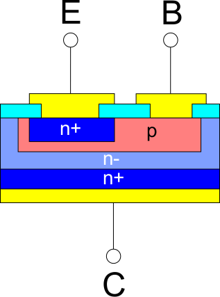
A transistor is an electronic component that is basically an on / off switch. A control signal at the input, the base, enables a current to flow between the two outputs called collector and emitter or not.
A simple transistor is the bipolar transistor, which consists of doped silicon, which has a higher conductivity than untreated silicon. Depending on the foreign material that is introduced into the silicon lattice, one speaks of n-doped (electron-rich) or p-doped (electron-poor) silicon. Bipolar transistors exist as npn or pnp transistors, the only difference being the direction of the current flow.
In the case of the npn transistor, a positive voltage is applied to the base, so that a small control current flows between the base and emitter. This current is amplified by the transistor by a fixed value, so that a larger current flows between the collector and emitter. The gain factor is determined by the external wiring with resistors. A bipolar transistor is therefore an analog current amplifier, as it is still used today in audio amplifiers.
- Schematic structure of a bipolar transistor with emitter (E), base (B) and collector (C). (Image: Wikipedia)
image 1 from 2
Via MOSFETs to the CMOS
For digital circuits you need two clearly separated voltage levels for the values 0 and 1, e.g. B. 0 V and 5 V. A suitable switch changes back and forth between these two voltage levels and does not assume any intermediate states. In order to keep losses as low as possible, the amplifier should have a negligible current flow for the switching process, which excludes bipolar transistors.
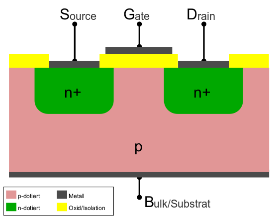
These requirements have been met through the development of field-effect transistors (FETs) that operate with practically no current flow. In FETs, the three connections are referred to as gate, source and drain. The gate of an FET is separated from the rest of the transistor by an insulating layer. If a voltage is applied to the gate, an electric field is created instead of a control current flow, which increases the conductivity between the source and drain. The FET therefore switches current-free. Since subsequent FETs also do not need a current flow to switch, it is sufficient to pass through the switching voltage of z. B. 5 V to operate entire circuits. A digital circuit consisting of a number of FETs is therefore theoretically lossless. The standard manufacturing technique for FETs consists of a combination of metals (M), insulating oxides (O) and semiconductors (S), which is why the technology for field-effect transistors is abbreviated as MOSFET.
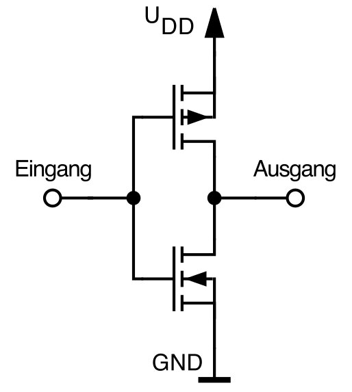
For a perfect digital circuit, however, a single transistor still has one disadvantage: when it is in the blocked state, the voltage at its output is not clearly defined. It is not the 5 V of the supply voltage, because it is blocked, but it is also not exactly 0 V (GND), as a line with 0 V would have to be passed through for this. This ambiguity in the blocked state is resolved by combining two oppositely doped MOSFETs. In a structure made up of an n-MOSFET and a p-MOSFET, the first transistor works as described above, while the second transistor passes through exactly 0 V whenever the first one blocks. Since the two transistors complement each other, one speaks of “Complementary MOSFET”, or CMOS for short. The CMOS technology enables clean digital signals with particularly low energy consumption and short switching times.
On the basis of this knowledge, the manufacturing techniques and the functionality of modern CMOS transistors will now be considered.
The goal of semiconductor manufacturing technology
The goal of semiconductor manufacturing technology is the ever smaller production of field-effect transistors, which means that increasingly complex circuits can be manufactured at lower costs, because each exposed mm² costs on the wafer. Further advantages such as increased switching speeds and reduced power consumption by the transistors are secondary effects of improved production. ComputerBase created a more detailed overview of semiconductor production in the clean room a few years ago in a self-experiment.
The production by photo-lithography basically builds up a transistor from the bottom up. Compared to a bipolar transistor, the structure of a CMOS transistor is very similar in the lower layers. These areas are achieved through the different doping of the silicon. A lithography step consisting of the application of photoresist, exposure and development is necessary for each doping. The special difference with the FET is the integration of a capacitor-like structure at the base, which collects charge carriers above or below the oxide layer (depending on the voltage). This means that two further lithography steps are necessary, in which, instead of doping, first the insulator and then the metal contact are applied.
On the next page: Advances and innovations in manufacturing I
Related posts:
 7-nanometer Nvidia GPU, TSMC will handle most of the production
  ASRock X299, a new BIOS allows you to install 2 TB of memory
  MSI Prestige X570 Creation Review: Test | Specs | Hashrate
  Radeon RX 5500 XT, PCI Express 3.0 castrates performance?
  An overclocker ran 1TB of RAM on an X299 motherboard limited to 256GB
  Best Review 2021: MSI MPG X570 Gaming Edge WiFi Under $250 ($200)