How to ‘Increase/ Max/ Optimize/ Tuning/ Boost’ Hashrate Radeon VII Mining + Gaming: Overclocking/ Ethash / Best Overclocking Setting – In this review, we will look at the 16 GB version of AMD’s Radeon VII reference video card.
The card is equipped with 2×8 Pin connectors and consumes from 180 watts to 320 watts depending on overclocking, miner and algorithm.
In stock, the card gives out ~ 90 Mh / s on the Ethash algorithm.
How to Increase Hashrate Radeon VII Mining: Specifications
| Specifications | Reference Radeon VII |
| video memory | HBM2 16GB |
| CPU frequency | Overclocking frequency: 1800 MHz |
| Technical process | 7nm |
| Energy consumption | From 180 watts to 320 watts |
| Power Connectors | 2x8Pin |
| Length | 27 cm |
| Noise | 52 dB |
How To 100Mh/s Radeon VII Mining ETHEREUM C-Mode in HiveOS!
Temperatures and internals
- Length – 27 cm
- Noise ~ 52 dB
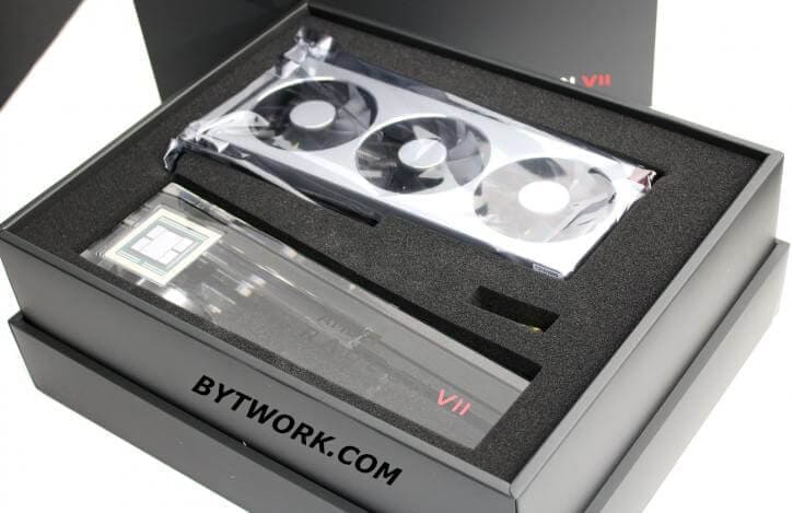
Let’s start the review of the video card with the bundle. The Radeon VII bundle consists of:
- Box
- Map
- Manual
So far, it is impossible to say exactly what the final configuration will be for users, since the card was sent to all reviewers in a special, exclusive configuration: card + stand.
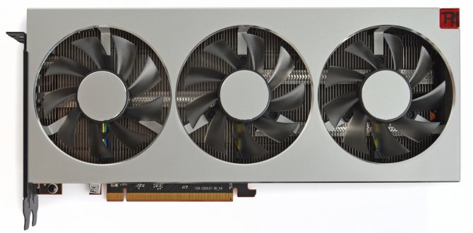
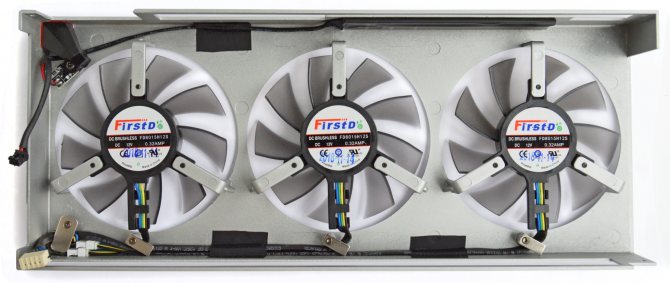
Next, let’s move on to coolers. The card is equipped with 3 medium-sized coolers with a diameter of 75 mm each.
In idle mode – 800 rpm.
Under load – 3.000 rpm and above.
Here we can immediately see a noticeable difference from the reference Vega 64 (turbine). Looking ahead, let’s say that this cooling system (3 fans) showed itself much better than the cooling in Vega 64.
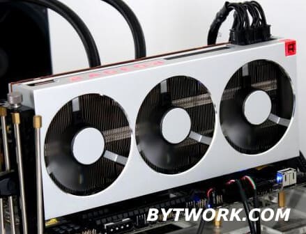
Note that the coolers are the same as in SAPPHIRE video cards, but this is not surprising, since this company makes reference samples for AMD.
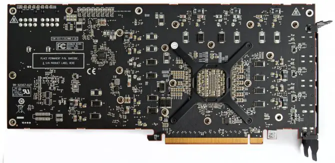
Let’s move on to the back of the video card, namely the backplate. This model has it. In the backplate itself, we can see numerous slots, as well as a cutout (hole) in the GPU area. Note that the backplate of this model is installed correctly and is well ventilated.
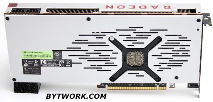
Recall that the backplate does not serve as a cooling element, moreover, on the contrary, if it is installed illiterately, the card will heat up even more. The backplate serves as a kind of protection for the back of the PCB and adds rigidity to the structure.
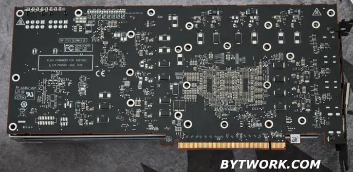
With the backplate removed, we can see the back of the PCB.
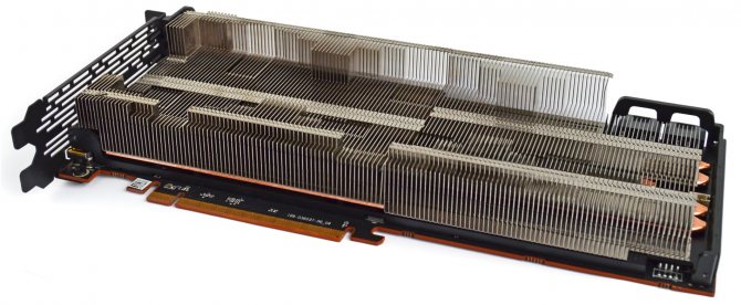
Finally, let’s move on to the analysis of the video card, namely the printed circuit board and the internal cooling system (let’s start with it).
The radiator grill itself is relatively small, especially for a video card with such power consumption.
Note that the direction of the grille ribs and the closed shape of the casing itself allow you to blow air only perpendicular to the motherboard.
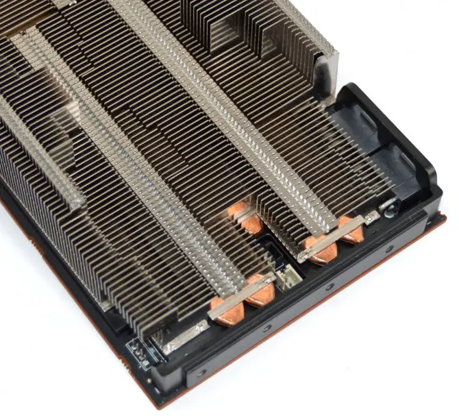
5 flattened heat pipes 10 millimeters wide pass through the radiator grille.
A metal plate is attached to the grille, which is in direct contact with the printed circuit board. Here we can see the thermal stickers and the copper plate.
Note that the Radeon VII does not use thermal paste, and a special thermal sticker is applied to the copper base. When parsing the card, it breaks and replacing it with thermal paste seems to us not the best option. This is due to the fact that the thermal sticker for Hitachi TC-HM03 GPU has a thermal conductivity (25-45 W / m K), which is significantly higher than that of the highest quality thermal pastes (12.5 W / m K).
Let’s move on to the circuit board itself. She looks very good.
Thermal stickers are glued to the VRM, GPU and memory.
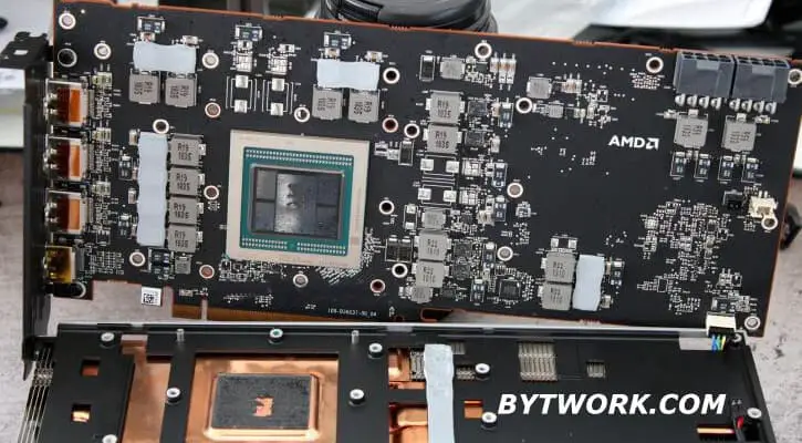
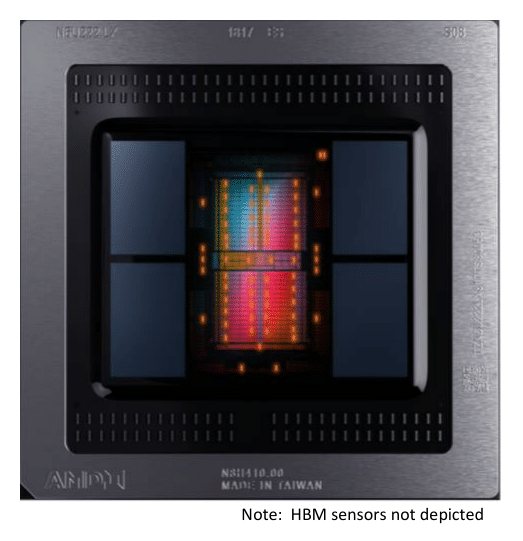
The memory is presented in the form of 4 dies around the GPU – this is 16 GB HBM2 from Micron.
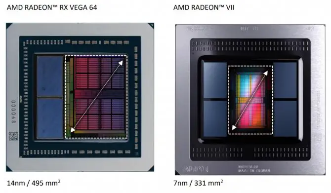
As for the GPU, Vega has made a huge leap from 14nm FinFET to 7nm. The Vega 20 GPU is manufactured by Taiwanese company TSMC.
Let’s move on to thermals.
Thermal imager
All thermal images were taken under maximum load for a general idea and understanding of the cooling system with a slight overclocking of the core and memory.
| measuring point | Degrees Celsius) |
| M1 | 59.8 |
| M2 | 49.5 |
| M3 | 48.2 |
| M4 | 34.4 |
| M5 | 37.7 |
By installing the thermal camera on top, we get the following results:
The hottest point – M1 (60 degrees) is located above the GPU. This is a very good result.
We also note that hot air, judging by the thermal images, does not linger and is actively dissipated by the fans.
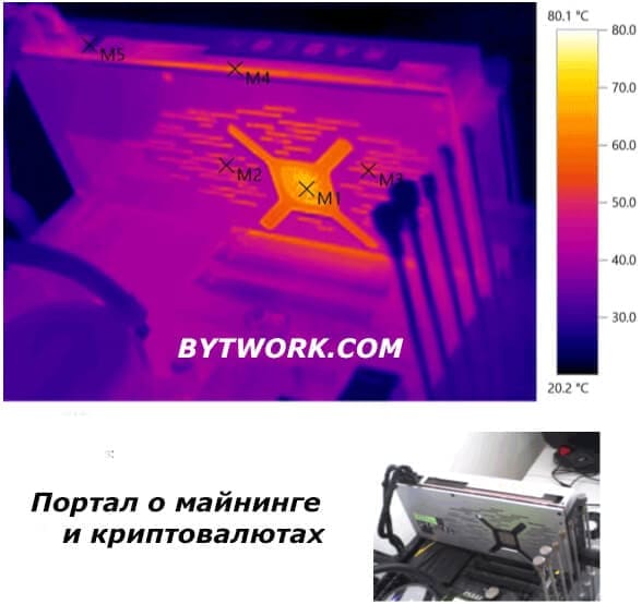
| measuring point | Degrees Celsius) |
| M1 | 67.8 |
| M2 | 42.8 |
| M3 | 51.4 |
| M4 | 57.8 |
| M5 | 31.4 |
By installing a thermal camera from the back of the video card (from the backplate), we get the following results:
The hottest point – M1 (GPU temperature) is at around 68 degrees. This is a good result, considering that the card consumed at the time of the test from 290-300 watts.
However, it should be noted that the card stands alone in an open stand and is well ventilated.
In any case, we are seeing a noticeable jump in the cooling system of the new video card from AMD.
Review and testing of the video card Radeon VII. Faster, cooler, more economical?!
AMD is back in the class of top devices. Last fall, NVIDIA introduced a series of GeForce RTX graphics cards that significantly raised the bar for performance. All this led to the downgrading of the Radeon RX Vega, and the entire older market segment was captured by NVIDIA. But after the announcement of AMD Radeon VII, consumers will have an alternative and a choice.
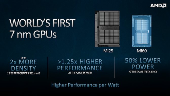
The new Radeon VII graphics accelerator is the successor to the Radeon RX Vega and uses a GPU based on the second generation Vega architecture. And this is the first gaming accelerator with a GPU, made according to the 7nm process technology. Hence the name Radeon VII. At the same time, the newcomer is an analogue of the dedicated Radeon Instinct MI50/MI60 series computing accelerators, which were introduced back in November.
A key feature of Vega is the combined structure, when the graphics processor and memory blocks are located on a single substrate. The pioneer here was the Radeon R9 Fury X accelerator, and AMD continues to develop and improve such GPUs. In the first generation Vega, two HBM2 memory blocks were used, which provided data exchange over a common bus with a width of 2048 bits. The Vega 30 processor has four HBM2 blocks, i.e. the bus width is already 4096 bits, and the total memory is 16 GB.
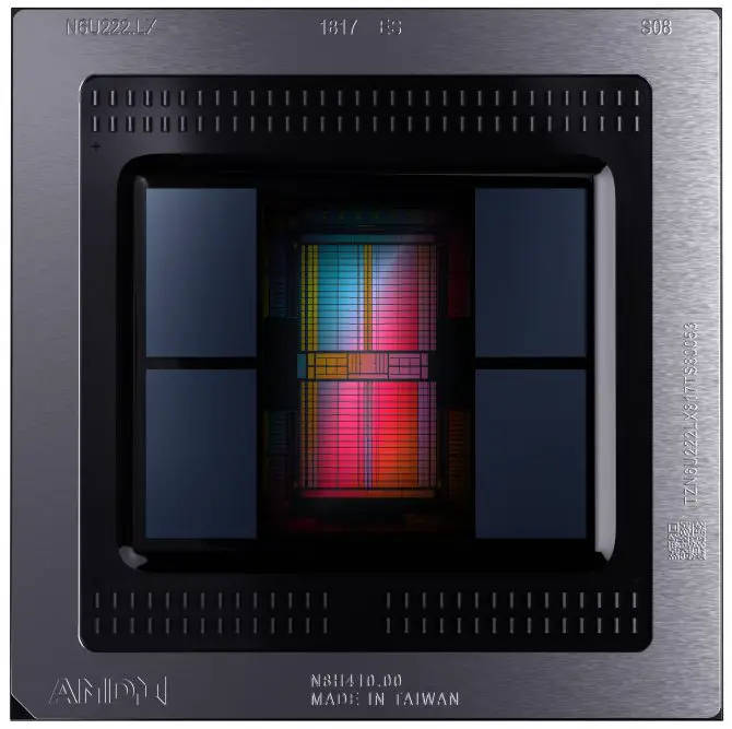
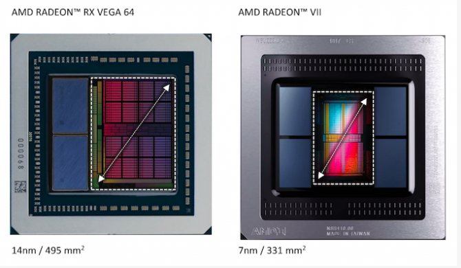
The transition to a new technical process provided a reduction in the die area to 331 mm² instead of 495 mm² for Vega 10. This made it possible to place four memory stacks instead of two.
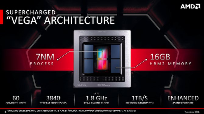
The structure of the GPU itself has not undergone major changes relative to Vega 10, and for a detailed description, you can refer to our old review. The GPU consists of 64 large Compute Units (CUs) with 64 stream processors each. But the Radeon VII has 60 CUs active and 3840 stream processors. It seems to be some kind of compromise solution to achieve higher frequencies and a reasonable TDP.
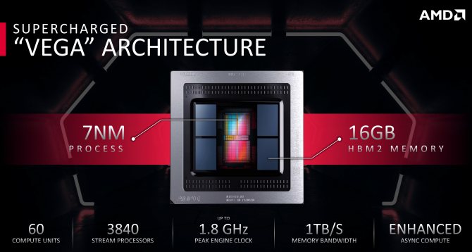
Base core clock is now 1400 MHz with Boost 1750 MHz. For the Radeon RX Vega 64, this was a combination of frequencies 1274/1546 MHz. For Vega-based Radeon GPUs, the Boost value indicates the average frequency under typical load. The maximum possible value for Radeon VII reaches 1800 MHz.
Memory bandwidth reaches a record high of 1 TB / s. The frequency of memory blocks is 1000 MHz, the effective value of DDR is 2000 MHz. Since the Radeon RX Vega 64 had an effective memory frequency of 1890 MHz, the increase in memory bandwidth is more than doubled. This is definitely impressive. However, outside of such a powerful memory acceleration, no other significant architectural improvements have been announced for Vega 20.
| Video adapter | Radeon VII | Radeon RX Vega 64 | Radeon RX Vega 56 |
| Core | Vega 20 | Vega 10 | Vega 10 |
| Number of transistors, million pieces | 13200 | 12500 | 12500 |
| Process technology, nm | 7 | 14 | 14 |
| Core area, sq. mm | 331 | 495 | 486 |
| Number of stream processors | 3840 | 4096 | 3584 |
| Number of texture blocks | 240 | 256 | 224 |
| Number of render units | 64 | 64 | 64 |
| Base core frequency, MHz | 1400 | 1274 | 1156 |
| Boost frequency, MHz | 1750 | 1546 | 1471 |
| Peak core frequency, MHz | 1800 | 1630 | 1590 |
| Memory bus, bit | 4096 | 2048 | 2048 |
| Memory type | HBM2 | HBM2 | HBM2 |
| Memory frequency, MHz | 2000 | 1890 | 1600 |
| Memory size, GB | 16 | 8 | 8 |
| Supported version of DirectX | 12 (12_1) | 12 (12_1) | 12_1 |
| Interface | PCI-E 3.0 | PCI-E 3.0 | PCI-E 3.0 |
| Power, W | 300 | 295 | 210 |
Radeon VII is presented as a competitor for the GeForce RTX 2080, i.e. NVIDIA’s top video card is once again left without a rival. The cost of the novelty is also at the level of the GeForce RTX 2080. At the same time, the Radeon VII has a record amount of memory of 16 GB instead of 8 GB from a direct competitor, and even the GeForce RTX 2080 Ti has only 11 GB. Since the Radeon VII is a top-tier solution, it is designed for high-definition games, including 4K and ultra-wide formats. Under such conditions, memory usage can be extremely high. According to AMD, some new games (Metro Exodus, The Division 2) can load up to 11 GB in 4K, and Far Cry 5 with HD textures uses up to 12.9 GB. And if we consider the trend towards a gradual increase in system requirements, then soon we can see games with even higher demands. With no memory limits
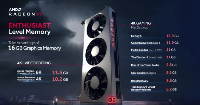
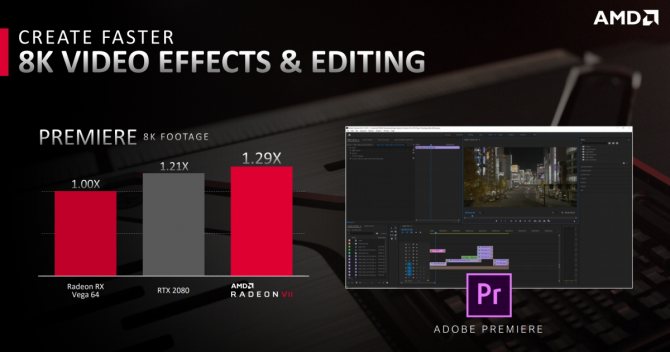
Radeon VII is not only a gaming accelerator, it is also a device for content creators and professionals. In particular, it is a powerful accelerator for video editing or rendering. When working with 8K video, the advantage of the new flagship over older solutions is 27-29% in DaVinci Resolve and Adobe Premiere. And here, too, a high amount of memory is useful, because Adobe Premiere consumes 10-11 GB when working with 4K / 8K content.
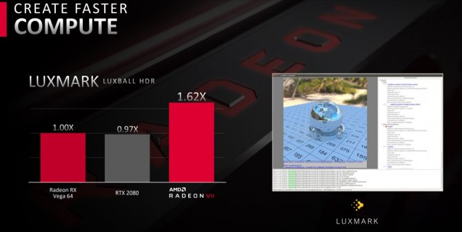
In OpenCL based computing, the gap with the old Radeon RX Vega 64 can be very significant. So, in the specialized benchmark LuxMark, the advantage of Radeon VII is up to 62%.
In Blender, rendering with a beginner is 27% faster.
The new video adapter can be used in highly specialized calculations. However, it is slightly clipped in FP64 double precision calculations relative to the original Radeon Instinct. In FP32, Radeon VII delivers 14.2 TFLOPS, while in FP64 it is already 3.5 TFLOPS. But these are still very high figures for such a price category, where only non-professional solutions are available.
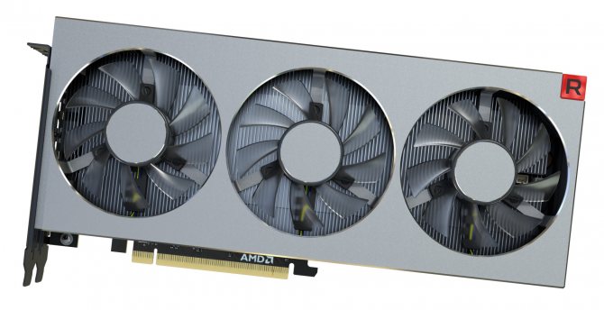
AMD engineers this time thoroughly approached the issue of cooling. The usual “turbine” can no longer cope with powerful graphics accelerators. Therefore, Radeon VII uses a new air-cooling system with a large heatsink and three fans.
Read more about the design features of the video card in the next section.
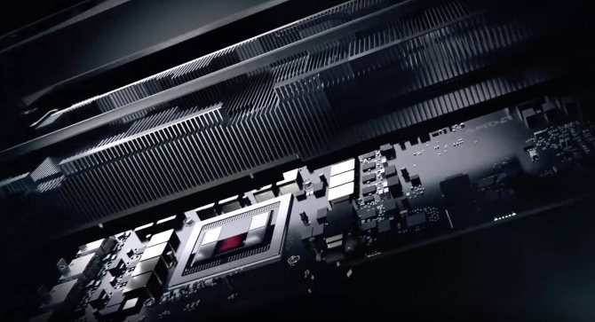
AMD Radeon VII
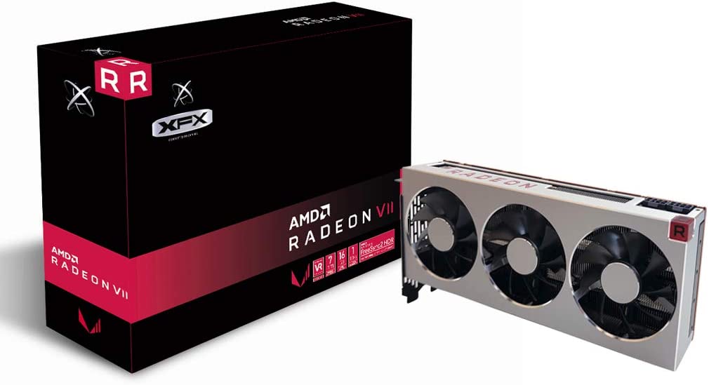
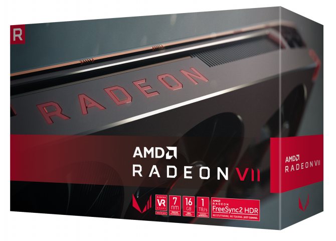
The video card comes in a large bright box.
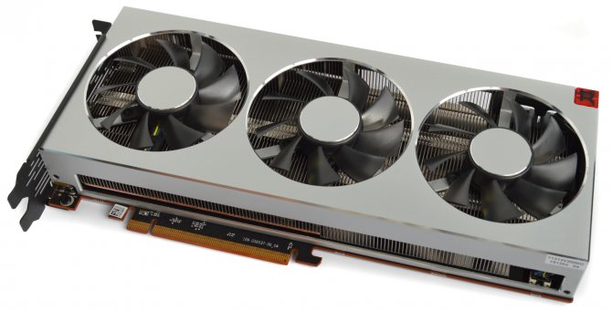
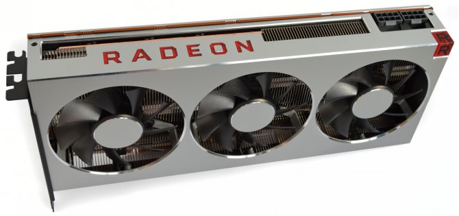
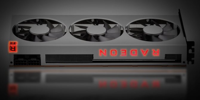
The Radeon VII looks simple but very solid thanks to its silver chassis and three fans.
The dimensions of the flagship can be called standard. The length is about 27 cm, the thickness is the usual two slots.
The reverse side is covered with a metal plate with a small perforation and an open area under the GPU chip.
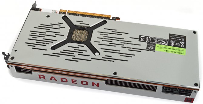
There are two eight-pin power connectors in the corner. On the side of the case there is a large inscription Radeon.
The Radeon inscription and the cube in the corner with the letter R are illuminated in red.
Three DisplayPort ports and one HDMI are provided for image output.
If we dismantle the silver case, we will see a radiator that occupies all the free space.
Along the edges of the radiator has protrusions in the form of steps. Niches between these protrusions are occupied by fans. That is, the entire available volume is used to expand the scattering area.
The copper heat pipes under the plates are also clearly visible. In the area of the GPU, you can see the evaporation chamber with a large base. And the whole structure is recessed into a black base.
For blowing, three fans with an impeller diameter of 75 mm are used. Their marking is FirstD FD8015H12S.
Alas, there will be no complete analysis, there are certain restrictions on this. But it should be noted the presence of a special graphite thermal pad for the GPU. This thermal interface provides high thermal conductivity and good contact in case the height of the GPU die and memory crystals differ slightly. And since it is subject to destruction and a replacement cannot be found, it is really better not to disassemble the video card.
You can look at the back side of the PCB, but all the main elements are placed on a different surface. The plate here performs only a protective function, there are no thermal pads under it.
According to the available slides, the PCB resembles a board from the Radeon RX Vega 64, where the power phases are soldered around the perimeter of the GPU.
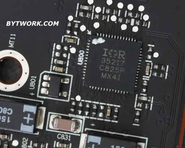
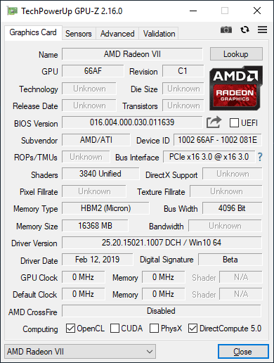
The set of software tools for working with Radeon VII is still limited. The GPU-Z utility detects the device and some parameters, but does not provide complete information.
Monitoring of frequencies and temperatures in third-party programs does not work yet. All necessary functions are available in the Wattman section of the Radeon Settings software package. AMD immediately provides the user with all possible settings, allowing you to adjust various parameters, control fans, and even overclock the video card. Therefore, you can do without additional utilities.
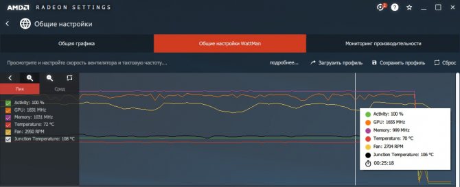
To evaluate the temperature and noise characteristics, we used the Final Fantasy XV Windows Edition benchmark. Based on the results of a continuous 12-minute test, he warmed up the video card to 71 ° C at a resolution of 2560×1440 and up to 72 ° C at a resolution of 3840×2160. The core frequency ranged from 1700-1780 MHz at lower resolutions and from 1650-1770 MHz in 4K mode. It is noteworthy that the peak values are higher than the 1800 MHz declared in the specifications, up to 1893 MHz. The memory peak values are also higher than the declared frequency, but at each marked point we see the prescribed 1000 MHz.
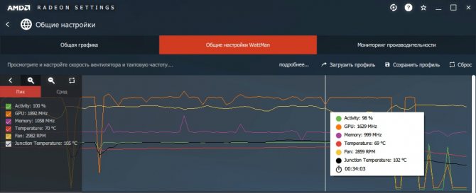
For clarity, let’s add another screenshot with monitoring data during the Shadow of the Tomb Raider tests in 4K, where drawdowns up to 1630 MHz are visible. But mostly frequencies above 1700 MHz.
The screenshots show that the maximum fan speed is approaching 3000 rpm, the average level is 2700-2800 rpm. The noise in such conditions is high, but the temperature for such a powerful GPU is extremely low. These specifications were obtained on an open bench at 23°C indoors. For comparison, it should be noted that our Radeon RX Vega 64 air-cooled in similar conditions easily warms up to 80-85 ° C. The GeForce RTX 2080 Ti Founders Edition also approaches 84°C under these conditions.
With such excellent temperatures, you can try to achieve lower noise levels through manual settings and lower fan speeds. However, it must be understood that the manufacturer had a certain motivation, trying to ensure a comfortable temperature regime and complete stability of the device in any operating conditions. The heating of a video card inside a case with poor ventilation can be noticeably higher, and all manipulations with the settings must be done carefully.
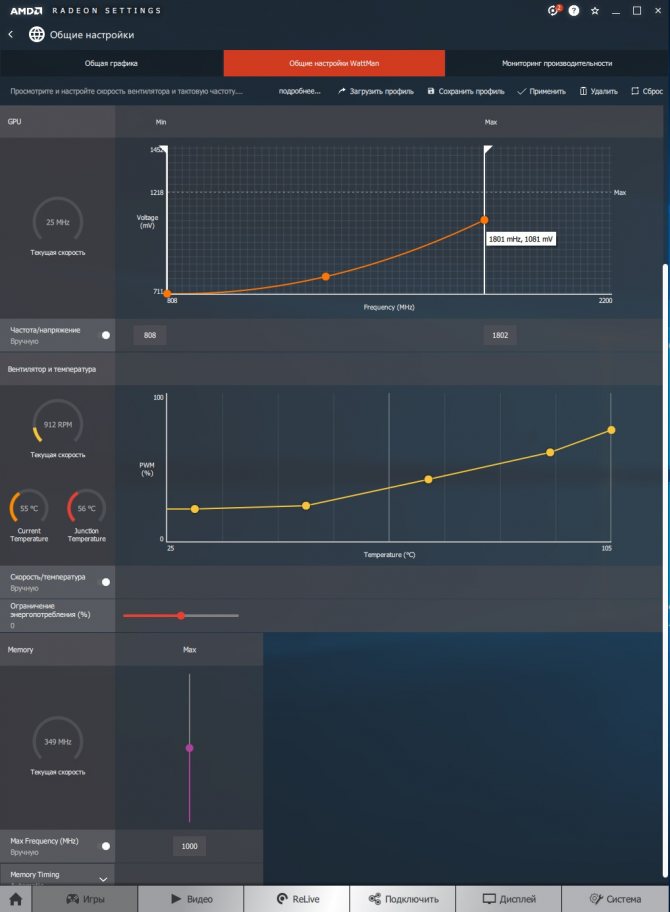
Let’s talk more about the settings. The Wattman menu has a slightly changed interface for managing video card settings. It is now possible to change frequencies and corresponding voltages through a curve for which extreme and intermediate points are set. And it’s actually very simple, just change the extreme values to change all the values. We moved the extreme point along the X axis – we got an increase in frequencies. We moved the point up along the Y axis – we got a smooth increase in stresses for all intermediate values. The fan control algorithm is also set through a curve with adjustable temperature points. The power limit can be increased by 20%. Memory overclocking available. There is a GPU and memory auto-overclocking mode, timing optimization and automatic Undervolt GPU tuning.
We tested the latter mode using the Final Fantasy XV benchmark as an example. By selecting Undervolt GPU, you allow the system to automatically switch the graphics card to lower voltages, which will reduce power consumption and heat. When fixing all frequencies in auto mode, we got a slight increase in performance, about 1%, with a decrease in peak power values in the selected test by about 15 watts. A very good result, but it will depend on the load in each particular application.
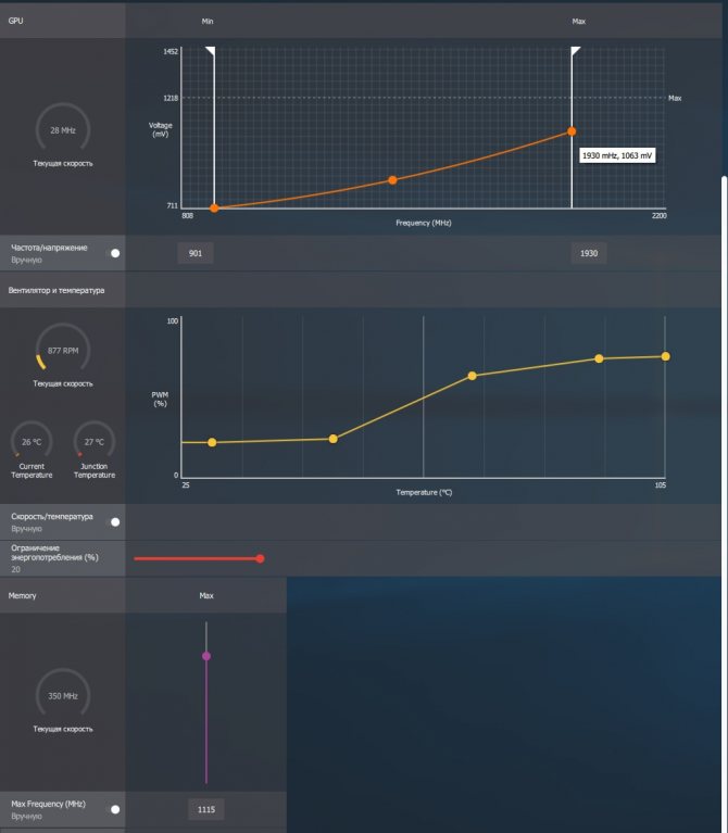
It’s time to move on to overclocking. After a series of tests, we settled on the upper value of the GPU frequency of 1930 MHz. Increasing the maximum Boost point further resulted in crashes. Notably, increasing the voltage did not improve stability for heavy tests. It should be recalled that the overclocking of the Radeon RX Vega was to find stable frequencies and, if possible, reduce the voltage relative to the initial values. And we went that route for Radeon VII. The default for 1800 MHz was 1.08 V, for 1930 MHz it was reduced to 1.06 V, then stability problems also began. The memory was overclocked to 1115 MHz (2230 MHz). Increased power limit and fan speed.
At the selected settings in Final Fantasy XV in 4K, the main frequency range was approximately 1800-1900 MHz with occasional drops below 1800 MHz.
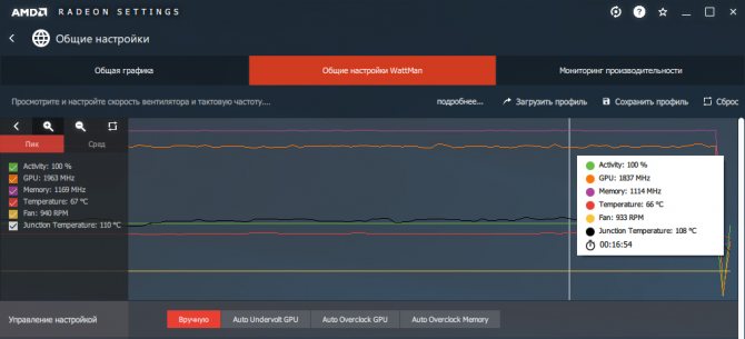
When changing the fan settings, an error appeared with speed monitoring, so you should not look at the low numbers in the screenshot above. In reality, overclocking is associated with high noise. But this is not the sad situation when the Radeon RX Vega 64 had to bring the turbine to the maximum. Here you can work with an overclocked video card without risk to your ears. In terms of cooling, progress is very serious.
Radeon VII VS Radeon RX Vega 64 VS GeForce GTX 1080 Ti VS GeForce RTX 2080: Comparison
Let’s compare the performance of Radeon VII with Radeon RX Vega 64, GeForce GTX 1080 Ti and GeForce RTX 2080 Founders Edition. These competitors have been tested at nominal and overclocked. Also, for clarity, let’s add the results of the GeForce RTX 2080 Ti Founders Edition in nominal value. NVIDIA Founders Edition video cards have some Boost acceleration relative to the simplest models, and this should be taken into account when comparing the results.
| Video adapter | Radeon VII | Radeon RX Vega 64 | GeForce RTX 2080 Ti FE | GeForce RTX 2080 FE | GeForce GTX 1080 Ti |
| Core | Vega 20 | Vega 10 | TU102 | TU104 | GP102 |
| Number of transistors, million pieces | 13200 | 12500 | 18600 | 13600 | 12000 |
| Process technology, nm | 7 | 14 | 12 | 12 | 16 |
| Core area, sq. mm | 331 | 486 | 754 | 545 | 471 |
| Number of stream processors | 3840 | 4096 | 4352 | 2944 | 3584 |
| Number of texture blocks | 240 | 256 | 272 | 184 | 224 |
| Number of render units | 64 | 64 | 88 | 64 | 88 |
| Core frequency, MHz: Base-Boost | 1400–1750 | 1274–1546 | 1350–1635 | 1515–1800 | 1480–1582 |
| Memory bus, bit | 4096 | 2048 | 352 | 256 | 352 |
| Memory type | HBM2 | HBM2 | GDDR6 | GDDR6 | GDDR5X |
| Memory frequency, MHz | 2000 | 1890 | 14000 | 14000 | 11008 |
| Memory size, GB | 16 | 8 | 11 | 8 | 11 |
| Supported version of DirectX | 12 (12_1) | 12 (12_1) | 12 (12_1) | 12 (12_1) | 12 (12_1) |
| Interface | PCI-E 3.0 | PCI-E 3.0 | PCI-E 3.0 | PCI-E 3.0 | PCI-E 3.0 |
| Power, W | 300 | 295 | 260 | 225 | 250 |
The table shows the official specifications for GPU frequencies. The graphs indicate the full range of frequencies, including peak Boost values.
test stand
The test bench configuration is as follows:
- processor: Intel Core i7-6950X (3,[email protected],1 GHz);
- cooler: Noctua NH-D15 (two NF-A15 PWM fans, 140 mm, 1300 rpm);
- motherboard: MSI X99S MPower (Intel X99);
- memory: G.Skill F4-3200C14Q-32GTZ (4×8 GB, DDR4-3200, CL14-14-14-35);
- system drive: Kingston SSDNow KC400 (512 GB, SATA 6Gb/s);
- secondary drive: WD Red 3TB WD30EFRX (3 TB, SATA 6Gb/s, 5400 rpm);
- power supply: Seasonic SS-750KM (750 W);
- monitor: ASUS PB278Q (2560×1440, 27 ″);
- operating system: Windows 10 Pro x64;
- Radeon VII driver: AMD Adrenalin Edition 19.2.2;
- Radeon RX Vega driver: AMD Adrenalin Edition 18.9.3 and 18.10.2;
- GeForce driver: NVIDIA GeForce 411.70 and GeForce 416.34.
Testing was carried out at resolutions of 2560×1440 and 3840×2160 according to the method described earlier. Additionally, tests were carried out in Assassin’s Creed Odyssey and Battlefield V. There was no full set of participants at the time of additional tests, therefore, there are no GeForce RTX 2080 in these games.
Test results
Assassin’s Creed Odyssey
Here the advantage of Radeon VII over Radeon RX Vega 64 is up to 25%. It also manages to bypass the GeForce GTX 1080 Ti by 8%. Overclocking provides 6-7% acceleration of Radeon VII.
Assassin’s Creed Origins
In Origins, NVIDIA solutions have more powerful positions, and the Radeon VII is slightly inferior to the GeForce GTX 1080 Ti. In high resolution 4K, the advantage over the Radeon RX Vega 64 reaches 25-27%.
Battlefield 1
In Battlefield 1, the hero of the review demonstrates a 26-30% lead over the Radeon RX Vega 64, almost as good as the GeForce GTX 1080 Ti. But this is in DirectX 11, but what is the situation in DirectX 12?
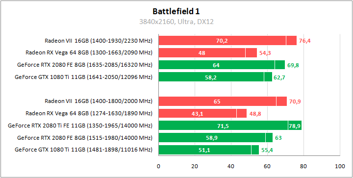
Everything changes dramatically. NVIDIA video adapters show a drop in fps, the Radeon RX Vega 64 also has a performance drop, but with a minimal difference. But the Radeon VII gets an unexpected acceleration, and after overclocking it almost catches up with the GeForce RTX 2080 Ti. Such an unexpected result that one can assume one of two things: a really strong speedup in the new API due to fast memory, or some kind of rendering error. The latter cannot be ruled out after last year’s situation with Kingdom Come: Deliverance, when AO did not work on AMD for several months. Here are just obvious visual differences this time we did not notice.
Battlefield V
In the new Battlefield, the Radeon VII has a serious advantage over the Radeon RX Vega 64 and a 23-30% lead over the old AMD representative. Acceleration gives an additional acceleration of 8-10%.
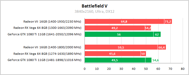
There are no surprises in DirectX 12. Fps drops by a few percent for all participants, the final ratio does not change.
Deus Ex: Mankind Divided
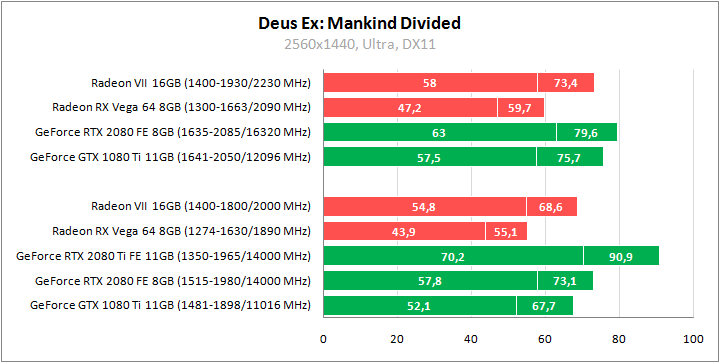
Radeon VII is 25% faster than its predecessor in Mankind Divided. At lower resolutions, it’s on par with the GeForce GTX 1080 Ti, and at 4K, it’s on par with the GeForce RTX 2080.
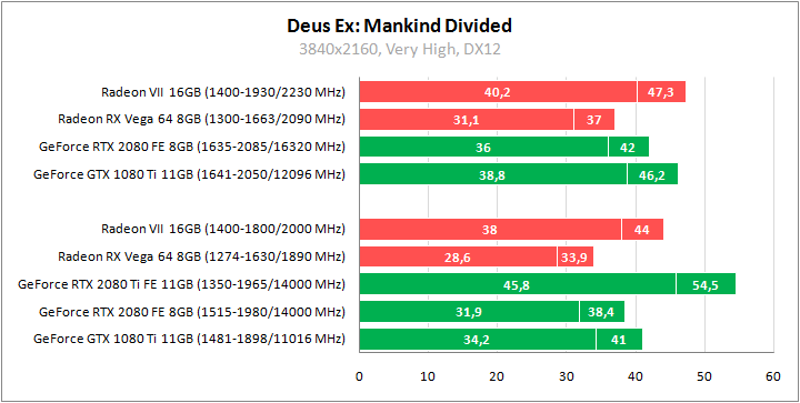
Switching to DirectX 12 provides acceleration and higher performance compared to the GeForce RTX 2080.
Fallout 4
The Radeon VII outperforms the GeForce GTX 1080 Ti and GeForce RTX 2080 in Fallout 4, with the biggest lead in high 4K. The difference with the Radeon RX Vega 64 reaches 29-31%. After overclocking to 4K, we manage to come close to the GeForce RTX 2080 Ti.
Far Cry 5
In both resolutions, Far Cry 5 slightly outperforms the GeForce RTX 2080. The difference with the simplest video adapter (not the Founders Edition) could be a couple of percent higher. Overclocking provides acceleration up to 8%.
Final Fantasy XV: Windows Edition
In Final Fantasy, the difference between Radeon VII and Radeon RX Vega 64 is 18-23%. Such acceleration is not enough to compete with NVIDIA representatives. In this game, the GeForce GTX 1080 Ti and GeForce RTX 2080 show the best results.
Grand Theft Auto 5
Radeon VII loses to the competitors of the green camp in GTA 5, although the difference in minimum fps is minimal. The gap with its predecessor is huge – the old Radeon RX Vega 64 is 33-38% inferior to the newcomer.
Kingdom Come: Deliverance
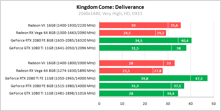
In Kingdom Come, Radeon VII is 16-19% faster than its predecessor. The minimum lag behind the GeForce GTX 1080 Ti and more noticeable with respect to the GeForce RTX 2080.
Mass Effect: Andromeda
In Andromeda, the newcomer AMD shows a 26-29% lead over the old Radeon, but still loses to competitors from NVIDIA. At 4K, the gap is slightly smaller, and the overclocked Radeon VII reaches the level of the GeForce GTX 1080 Ti.
Middle-earth: Shadow of War
The Radeon VII slightly outperforms the GeForce GTX 1080 Ti in terms of average fps in Shadow of War, although the situation is the opposite in terms of the minimum. GeForce RTX 2080 shows a slight advantage in nominal and overclocking.
Shadow of the Tomb Raider
In Tomb Raider, the considered Radeon VII is inferior to the GeForce RTX 2080 Founders Edition only in terms of the minimum fps. When compared with the simplest representative of the RTX 2080 series, this difference could completely disappear. So here we see equivalent solutions.
Strange Brigade
At the lower resolution of Strange Brigade, we can say that the Radeon VII is on par with its closest competitors. But at 4K, the AMD flagship not only confidently outperforms the GeForce RTX 2080, but also begins to approach the GeForce RTX 2080 Ti, minimizing the gap from the leader due to its overclocking.
The Witcher 3: Wild Hunt
In Witcher 3 at 2560×1440 resolution, the hero of the review shows a result between the GeForce GTX 1080 Ti and GeForce RTX 2080, but at 4K it is slightly inferior to the GeForce GTX 1080 Ti. The first mode uses HairWorks technology, and probably the heaviest mode reduces the benefits of NVIDIA solutions. The separation of Radeon VII from its predecessor reaches 27-29%. Acceleration from overclocking up to 8%.
Tom Clancy’s Ghost Recon: Wildlands
The Radeon VII is faster than the Radeon RX Vega 64 by 23-26%, slightly behind NVIDIA competitors. The difference with the latter is least noticeable in 4K resolution.
3DMark Time Spy
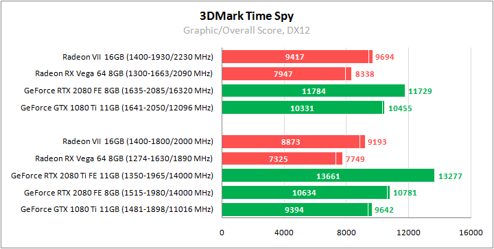
In this test, the difference between AMD solutions is only 21%. Radeon VII loses to GeForce GTX 1080 Ti by up to 6%, and with GeForce RTX 2080 Founders Edition the difference is almost 20%.
Energy consumption
A small preliminary comment on measurements. Due to the fact that the Seasonic SS-750KM test power supply could not ensure stable operation of the system with AMD solutions, another power source is used for them – Raidmax Cobra RX-800AE.
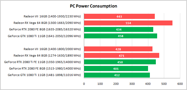
The Radeon VII was pleasantly surprised by the fact that its performance is noticeably lower than the power consumption of the Radeon RX Vega 64. In nominal terms, NVIDIA video adapters are slightly more economical, although the performance of the GeForce RTX 2080 Ti Founders Edition is already higher. In terms of overclocking, the difference between the Radeon VII, GeForce GTX 1080 Ti and GeForce RTX 2080 is negligible. You also need to take into account the probability of error due to different power supplies.
conclusions
Radeon VII is an evolution of the Vega architecture. Increased memory, increased bandwidth and high core frequencies provide a significant increase in performance. In games, the difference with the Radeon RX Vega 64 is at the level of 25-30%, sometimes lower, but sometimes higher.
This acceleration allows you to directly compete with the GeForce GTX 1080 Ti and GeForce RTX 2080. As for the advantages of the GeForce RTX 2080 in games, we need to remind you once again that the Founders Edition model with a slight factory acceleration appears in the tests. And in games under the Vulkan and DirectX 12 APIs, the advantage is often on the side of Radeon VII.
But most importantly, the new AMD flagship shows power consumption at about the same level as its direct competitors. We can say that the GeForce RTX 2080 is a little more economical, but the difference is negligible. Thanks to the new 7nm process technology, AMD has introduced a graphics accelerator that, in terms of the combination of characteristics, is not inferior to direct competitors. And if in the past generation, the hot temper of the Radeon RX Vega and high power supply requirements could scare off a potential buyer, now you have an equivalent choice between the Radeon VII and the GeForce RTX 2080.
It is worth mentioning that NVIDIA also has hardware ray tracing acceleration. But so far we have only two games that support this technology, and for a number of users this is not critical at all. It’s worth mentioning that NVIDIA also has hardware-accelerated ray tracing. But so far we have only two games that support this technology, and for a number of users this is not critical at all. It’s worth mentioning that NVIDIA also has hardware-accelerated ray tracing. But so far we have only two games that support this technology, and for a number of users this is not critical at all.
I would like to note the good efficiency of the new cooling system. A powerful cooler with a vapor chamber, heat pipes, a large heatsink and three fans maintains very moderate operating temperatures. Reference GeForce RTX models are hotter, not to mention the old Radeon RX Vega with the usual “turbine”. However, the noise level is high. An advanced user can achieve optimal performance through manual fan speed settings combined with corrective voltages.
There is the possibility of overclocking, which will provide an increase of 6-9%. If you combine overclocking with a slight decrease in voltage, then the increase in power consumption and heating will be small. However, all this is individual, the results may vary in different instances. Pleasantly, that AMD provides all the necessary functions for monitoring and configuration as part of its software, without requiring additional utilities. And the built-in controls are very convenient and intuitive.
In this review, our acquaintance with the Radeon VII will not be limited. Another material will be released soon with additional results and an extended list of test applications. Stay with us!
Memory and power consumption
The video card is equipped with 16 GB HBM2. Most often, as in this case, the memory is manufactured by Micron.
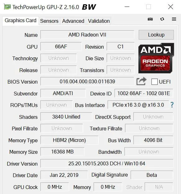
Note that some fields are blank as GPU-Z has not yet been updated to show all Radeon VII specifications.
This video card consumes from 180 watts to 300 (320) watts depending on the miner, algorithm and overclocking, where 75 watts goes through the riser, and the remaining 105 watts or 225 watts goes through 2×8 Pin connectors from the power supply.
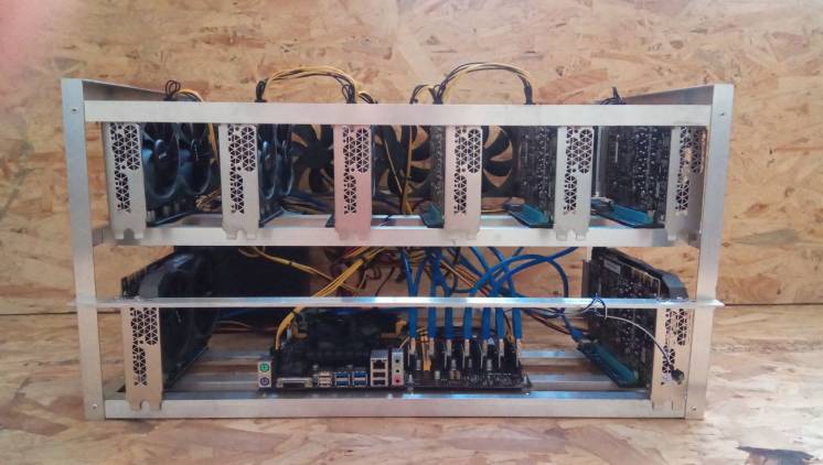
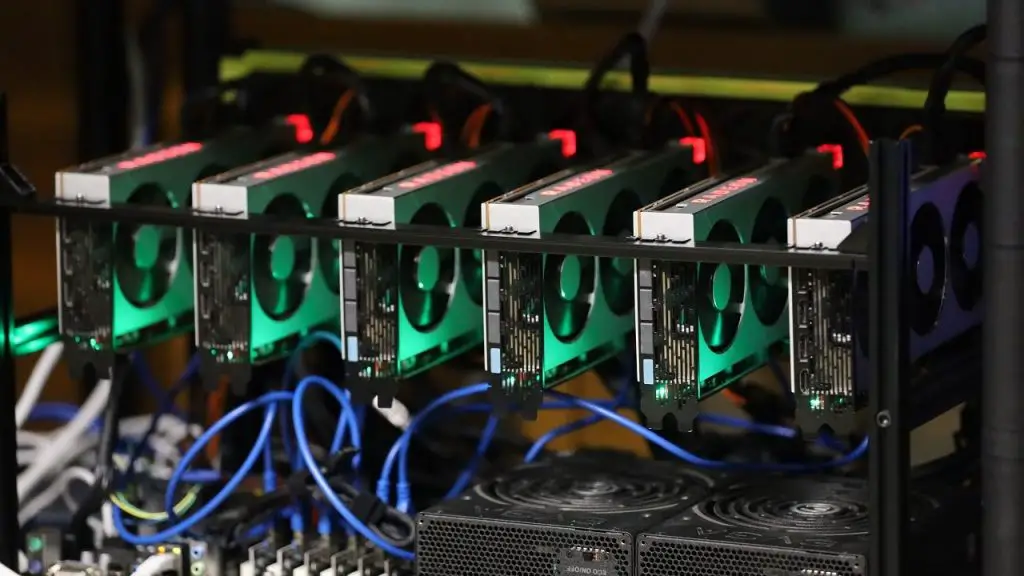
For a farm of 6 Radeon VII graphics cards and a connected system (motherboard, processor, hard drive (SSD)) you will need 1 unit of 2000 watts, or 2 power supplies of 1000-1100 watts.
You can find out how to power the farm with 2 power supplies on our website.
You can also choose an excellent block for mining on our website: the corresponding section contains detailed articles about different power supplies: their configuration, efficiency, drawdowns, ripple, analysis and much more.
This product has been designed to fit the most popular resolutions:
- Wide Quad
- Ultra HD.
- The reference board includes:
- 1 x HDMI (2.0b)
- 3 Display Ports
Note that there is no DVI connector, most likely vendors can embed it.
Specifications
| CPU |
| Radeon RX Vega 7 (Renoir) |
| Technical process |
| 7 p.m. |
| GPU frequency MHz |
| 1600MHz(Boost) |
| Stream Processors (Shading Units) |
| 448 |
| Texture Units (TMUs) |
| 32 |
| Raster Operations Pipelines (ROPs) |
| 8 |
| Memory type |
| system (DDR4) |
| (total graphics power) |
| 12-25W |
| DirectX version |
| 12.1 |
How much can you earn
Best of all, Radeon VII extracts Ethash, CryptoNightV8, CryptoNightHeavy, CryptoNightHaven algorithms. This can also include coins of ProgPow algorithms and sometimes NeoScrypt coins, but most often in the latter case this is due only to an increase in the rate of these coins or a temporary withdrawal of miners from their production.
In stock, the video card produces ~ 90 Mh / s on the Ethash algorithm.
The tests were completed on 02/08/2019, that is, the difficulties and prices for the given coins are relevant as of 02/08/2019.
>On the Ethash algorithm, the Ether coin, from 1 video card per day comes out:
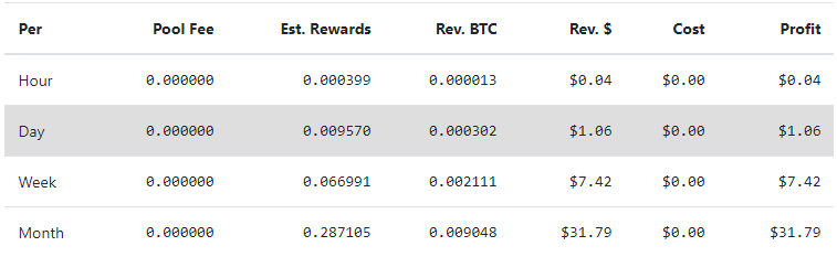
- Total coins – 0.00957 ETH.
- Amount in dollars equivalent to mined coins – $1.06
In general, not a bad result, considering that the card is not overclocked.
A little later we will post other tests in mining with this video card.
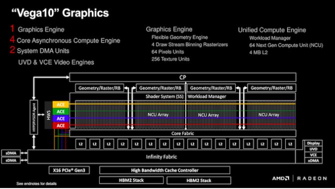
Under the hood of Vega 20: GCN at 7nm
While we’re already familiar with the Vega 20 through the release of the Radeon Instinct MI50 and MI60 server-class graphics cards, this chip’s entry into the consumer market marks the first 7nm gaming card. Rapid down-node hopping — this time from GlobalFoundries’ 14nm LPP to TSMC’s 7nm (CLN7FF) — has been AMD/ATi’s hallmark before, and here again AMD is rushing to release, bringing the product to consumers so early. In this case, all the attributes of Vega 20 are clearly intended for professionals and servers, although they also have advantages for games.
In the complicated history of the Radeon VII, Vega’s fate was especially mysterious. For starters, the 7nm Vega 20 GPU making its way to consumers so early came as a surprise. And while AMD only mentioned Vega 20 in relation to Radeon Instinct products – referring to its upcoming Navi architecture when referring to 7nm GPUs for gamers – AMD now claims that Radeon VII’s release to the consumer market was long overdue. Perhaps the same could be said for the Vega at 14nm+/12LP and the Vega 11 GPU (not to be confused with the 11 Ryzen 2400G Vega compute units), though this is hardly unusual given the nature of semiconductor development.
To be fair, AMD has been a bit lukewarm about the Vega ever since the launch of the RX Vega, which didn’t quite reach its goals. Even though the Radeon VII is in some ways a “Schrödinger chip”, it raises some interesting questions about 7nm. For example, AMD has already pushed back the timing of the sampling and launch of Vega 20 earlier. It turns out that the timing of the launch of Radeon VII is the earliest that could be for the heir to Radeon Instinct. Especially since with a die size of 331 mm2, these are not the small mobile SoCs that we have seen so far on TSMC 7 nm. Designed with compute/ML-centric enhancements in mind, equipped with 4 HBM2 stacks, and built on a mature and state-of-the-art 7nm node, the Vega 20 GPU doesn’t look like a card ready to make a good consumer price offering. And yet, thanks to a happy coincidence, it happened.
Vega 20 combines the updated GCN 5 architecture with a 7nm process, with 13.2V at 331mm2 transistors (compared to 12.5V at 496mm2 for Vega 10). As a rule, as the size decreases, the space savings are reinvested in more transistors. For a gaming graphics card, this could mean anything from more CUs and feature blocks, to redesigned layouts and increased data paths to increase frequency tolerance. The latter, of course, should provide a higher clock speed, and this choice was an important part of the Vega 10 design, where a significant number of transistors were used to achieve the required frequency response.
However, with Vega 20, most of the space saved was left “as is”: there is more free space on the chip. There are several reasons for this, some obvious and some not. To begin with, for a large high-performance GPU on a cutting-edge 7nm node early in the lifecycle, development and manufacturing are very costly. And it is likely that as the size increases, the cost will increase significantly, and the profitability of the product will decrease. And while TSMC’s 7nm process has only been publicly seen in mobile SoCs so far, Vega 20 appears to be using HPC-centric 7.5T libraries, as opposed to using 6T libraries designed for mobile SoCs.
But more importantly, the space saved allows two more HBM2 stacks to be placed on a similarly sized intermediate device. For current generation HBM2 densities and capabilities, the limit for a dual-stack chip is 16 GB of memory when using an “8-Hi” stack pair. But for a server-grade GPU – especially one focused on machine learning – a four-stack configuration is needed to provide 32 GB of memory and a wider 4096-bit bus. For the Vega 20, AMD has opted for just such a configuration, and is also releasing both 32GB (8-Hi) and 16GB (4-Hi) versions of the chip.
The Radeon VII, in turn, uses one of these 16GB chips. It should be noted that this is not the first 16 GB Vega card from AMD – they have already released a card with this amount of memory. This was a dedicated Vega Frontier Edition, but since its retirement, this is the first 16 GB graphics card release in the AMD Vega line.
Equipping a consumer card with 16GB of memory is a gamble on AMD’s part. And I suspect that’s one of the reasons AMD wants to capture some of the professional visualization market with the Radeon VII. When it comes to workstation usage and content creation tasks, a lot of VRAM is easy to sell as there are already tasks that can use all that VRAM and more. But for games, this is not the most reasonable suggestion, since games have more fixed requirements for VRAM, and so far there have been no such large cards, and developers have not yet begun to use the 16 GB VRAM resource. While on the other hand, the loud statement “this card has more than enough video memory” can have a serious impact on sales,
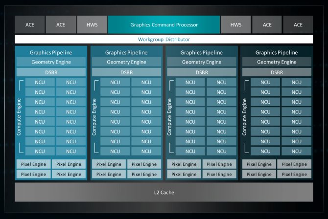
Returning to the design of the Vega 20, another step that AMD has taken to reduce the development complexity and cost of 7nm is to stick to an already known architecture. AMD added some small optimizations compared to Vega 10, but they didn’t risk a major redesign. In fact, this is the logic of the tick step of the famous tick-tock strategy of Intel. In fact, Vega 20 is such a direct successor to Vega 10 that, apart from the number of memory controllers, the number of other functional blocks is the same. The GPU integrates 64 CUs and 256 texture units divided into 4 Shader Engines, as well as 64 ROPs and an AMD GPU.
(I should add that in following their plan, AMD is also carefully avoiding the issue of shader engine scaling. The nature of the 4 Shader Engine limit has remained unclear in recent years, but with Vega there have been hints of going beyond these limits with improved load balancing with “intelligent workgroup distributors” (IWD). Regardless, setting up and redesigning a balanced 4+ SE configuration is a difficult task, and doesn’t make sense if AMD plans to make fundamental changes to GCN.)
So on an architectural level, the Vega 20 is a purely evolutionary design. But with that said, there’s a bit more “evolution” to it than just downsizing the tech node. The combination of these improvements means that in practice the Vega 20 should be slightly faster than the Vega 10 when running at the same clock speed.
The most notable improvement here is the extra memory bandwidth; twice as much per ROP, texture unit, and ALU than Vega 10. This is especially good for ROPs, which traditionally need a lot of bandwidth. Not stopping there, AMD has also made some improvements to the Core Fabric that connects memory to ROP (among other things). Unfortunately, AMD does not want to divulge what these improvements are, only confirming that there are no changes to the cache among them.
Another piece of the puzzle is that AMD has added new instructions and data types that will speed up machine learning in some cases. AMD hasn’t given us full details, but in general we do know that they have added support for the INT8 and INT4 data types, which are useful for low-precision inference scenarios. AMD also added the FP16 dot product, which is stored as the result of FP32. This is a rather specific scenario that is useful for some machine learning algorithms because it gives higher result accuracy than the FP16-in / FP16-out dot product.
Speaking of data types, AMD has also significantly increased the performance of FP64 for Vega 20. As a base architecture, GCN allows GPUs to be built at 1/2 to 1/16 the speed of FP32. For pure consumer GPUs, this has always been 1/16. However, for GPUs that carried a multifunctional load as server-oriented chips, 1/4 and 1/2 speeds were available. Vega 20, in turn, is the first ½ FP64 processor from AMD since Hawaii in 2013. This means that while its overall FP32 performance gain over Vega 10 cards isn’t as noticeable, its FP64 performance is much better: more than 8x over RX Vega 64 (theoretically). Of course, as a consumer card,
But when it comes to video blocks and display controllers, AMD has made only minor updates. Officially, the display controller (DCE) has been updated to version 12.1, while the version of the unified video decoder (UVD) is 7.2, and the version of the video coding engine (VCE) is 4.1. No additional encoding or decoding support has been added compared to Vega 10. We also found Display Core Next blocks from Raven Ridge and Video Core Next 1.0, so this may be the last architecture that these ASICs honor with their presence.
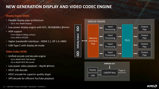
Function block wrapping is a new SMU style discussed in recent Linux kernel patches. Another feature is improved thermal monitoring, now the number of temperature diodes has been doubled to 64 sensors. As a consequence, AMD has now completely switched to node temperature monitoring instead of edge monitoring. Node temperature measurements were still used in Vega 10 (displayed as ‘hotspot’ temperature), but Vega 20 completely switched to node temperature measurement for all cooler speeds, turbo frequencies and the like. The result is more accurate reporting, as well as the marginal 1-2% performance gain AMD claims in internal testing.
The updated SMU, as a consequence of the above, has the following effect: temperature, clock speed and related GPU metrics are no longer read through registers, but are instead retrieved directly from the SMU. Naturally, this breaks compatibility with third-party utilities (like GPU-Z), and while AMD has already notified some developers of the changes, applications will need to be updated to use AMD’s new API calls.
Finally, since this is AMD’s first high-end Vega chip since the original Vega 10 in 2021, there are a few questions surrounding certain forward looking Vega hardware features. Information from AMD was not always clear, resulting in these features becoming a constant source of confusion for consumers.
With Vega 20, AMD doesn’t seem to be going to change things. That is, there was no further development by AMD regarding primitive shaders. Primitive shaders still have to be explicitly defined by developers, which means that the full potential of Next Generation Geometry (NGG) Vega 20 is not used (although it should be noted that the Intelligent Workgroup Distributor option was always enabled).
Meanwhile, AMD Vegas 10 already used the Draw Stream Binning Rasterizer (DSBR), and there were no changes here; the feature is enabled for an unspecified list of games. According to a quick check on Rapid Packed Math (rapid FP16), it is used for two famous games: Far Cry 5 and Wolfenstein II.
What coins can be mined?
As mentioned earlier, Ethash and CryptoNightV7 algorithm coins are best mined. Also, Lyra2REv2 and CryptoNightHeavy algorithms sometimes drip well.
Next are algorithms that bring a little less profit per day, but they can still be considered for mining: NeoScrypt, X16R, X16S.
Mined coins
| Algorithms | coins |
| Ethash | Ethereum, Ethereum Classic, Ellaism, Metaverse, Expanse, Krypton, Ubiq, Soilcoin, Shift, Pirl, Musicoin, Akroma, Callisto, DubaiCoin, Nilu, MIX, Goldiam, MOAC, Ether1, EtherSocial, WhaleCoin |
| NeoScrypt | Crowdcoin, Dinero, Feathercoin, GoByte, Halcyon, Innova, Vivo, Trezarcoin, Orbitcoin, Phoenixcoin, 01 Coin, Agena, Airin, Akencash, Banq, Cerberus, CharmCoin, Coin2Fly, CoreZ, Desire, GoaCoin, HashRental, IQ Cash, Ignition, Kicker Romm, LuckyBit, Masterbit, Momo Cash, NyxCoin, Onex Cash, Qbic, Qyno, Rapture, Sigil, SimpleBank, Sparks, SunCoin, SuperLumic, Uniform Fiscal Object, ZCore, Zixx |
| CryptoNightV7 | BBSCoin, Citadel, DigitalNote, Elya, IntenseCoin, Parsicoin, NXB, MoneroV, Lethean, Kepl, Quantum R L, Superior Coin, Wownero |
| CryptoNightV8 | Coin, Graft |
| TimeTravel10 | Bitcore |
| Lyra2REv2 | Monacoin, Galactrum, Rupee, Straks, Vertcoin, Verge, Absolute, Exvo, HanaCoin, Kreds, MTI Coin, WeyCoin |
| X16R | Ravencoin, Motion, GPUnion, Gravium, Help The Homeless, Hilux, MoonDEX, XChange, Stone Coin, Sovereign, Proton Coin, OPL Coin, xGalaxy |
| X16S | Pigeoncoin, Rabbit, Reden, RESQ Chain |
| Lyra2z | Actinium, Alpenschilling, Criptoreal, GINcoin, Infinex, MCT+, Taler, Respawn, STIM COIN, Taler, Vertical, Zcoin |
| CryptoNightHeavy | Alloy, Loki, Qwerty coin, RyoCurrency, zBucks |
under these algorithms you can on our website.
Comparison of Radeon VII with Vega 64
These video cards are noticeably very different from each other in such characteristics as performance, build quality, and cooling system.
Let’s start with performance. Radeon VII has become noticeably more powerful in mining, especially with a focus on memory-intensive algorithms. This is not surprising, because we got a noticeable increase from 8 to 16 gigabytes of fast HBM2 memory.
In terms of build quality, AMD did a very good job here too: the card is made of good materials.
The cooling system has become much better. With the transition from turbine to triple cooling, with the addition of high-quality thermal pads for the GPU and memory instead of thermal paste, we got a card with very good cooling, especially considering its high power consumption.
Related posts:
 How to overclock a graphics card in a laptop: MSI Afterburner – AMD & NVIDIA
  I7 4770K (OC) with RX 5700 XT: Hashate | |overclocking | Benchmark | 8 Games HD
  Red Dead Redemption 2: Overclocked FX 8350 and RX 5700 XT in FULL HD resolution
  AMD Radeon RX 6700 XT Mining: Hashrate | overclocking| Settings | Power Consumption
  How to increase: RTX 2060 vs 2060 Super Mining- Overclocking | HiveOS | Rave OS
  GTX 1080 Ti VS 1080 Mining: Overclocking | Profitability (Ether) | Power consumption