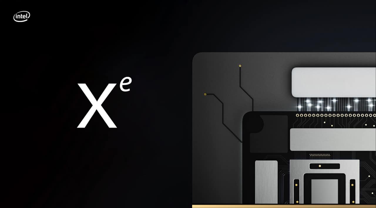
Intel has for many years competed with AMD for the throne for processors and later also graphics chips with the latter’s acquisition of the graphics maker ATI in 2006. Intel has also been involved in a minor battle with Nvidia, although then simpler graphics chips for laptops. In 2020, however, Intel will switch to a two-front war when the company returns to dedicated graphics cards with the Xe architecture.
This is done partly in dedicated graphics cards and integrated graphics circuits for consumers, but also in more solid donations for data centers and workstations. What goes by the code name Ponte Vecchio is Intel’s response to Nvidia’s and AMD’s graphics cards for data centers, where a heavy focus is on calculations of, among other things, artificial intelligence and machine learning. Intel’s graphics manager Raja Koduri has previously shown the solutions in pictures, and now he is on the move again.
BFP – big ‘fabulous’ package😀 pic.twitter.com/e0mwov1Ch1
– Raja Koduri (aRajaontheedge) June 25, 2020
Just like when Raja Koduri last unveiled images on Xe for data centers, the large processor packages are compared to an AA battery as a size comparison. The packaging, which is jokingly called “Big fabulous package, BFP”, applies the MCM structure where several circuits are connected to each other on one and the same substrate. The picture shows a total of three graphics packages that together make up the Xe family as stand-alone graphics cards.
At the top right is the smallest variant, which is probably about the Xe LP, which is the entry-level model for the middle-class graphics card. According to previous reports, this graphics circuit is equipped with 512 computing units (EU) and 4,096 stream processors with a TDP of 150 watts. To the left of the image is what is assumed to be Xe HP, which are circuits for data centers and workstations. These are said to consist of 1,024 EU units for a total of 8,192 stream processors and a TDP of 300 watts.
Leaked specifications for Xe where three levels of tiles or “tiles” determine the amount of EU units.
In the lower right corner is the massive circuit Xe XPC, which as the name suggests is about a graphics accelerator for supercomputers on exascale. According to reports, the Xe HPC is equipped with as many as 2,048 EU units and 16,384 stream processors, whose configurations are said to have TDP levels of 400 and 500 watts. The MCM structure in Intel’s Xe graphics cards is based on sets of tiles, where Xe LP consists of one tablet while Xe HP and Xe HPC consist of two and four tiles respectively.
The previously shown circuit appears to be the Xe HP package in the picture, which means that its real package surface of 3,700 mm² fades in comparison with the Xe HPC, which certainly justifies the packaging name “Big Fabulous Package”. The huge circuit is likely to be accompanied by a large cooling solution when it takes up space in high-performance supercomputers.
Intel has already launched Xe for consumers in the form of integrated graphics components in the “Tiger Lake” family processors. At the time of writing, the company has not announced a concrete launch plan for dedicated consumer graphics cards. Xe “Ponte Vecchio” for data center is manufactured on Intel’s 7-nanometer technology and will be released in 2021.
Read more about Intel Xe:
Related posts:
 Review & Test: Video card Gigabyte GeForce RTX 3060 Ti Gaming OC Pro
  AMD Radeon RX 5600 XT VS GTX 1660 Ti and RTX 2060: Review| Set-up| Hashrate
  Review of the KFA2 GeForce RTX 3060 Ti Core video card
  GIGABYTE GeForce RTX 3090 Gaming OC video card: Review| Specs | Set-up|
  INNO3D GeForce RTX 3090 iCHILL X4 video card review: Test | Config | Hashrate
  ROG Strix GeForce RTX 3070 OC Review: Test | Specs | Hashrate