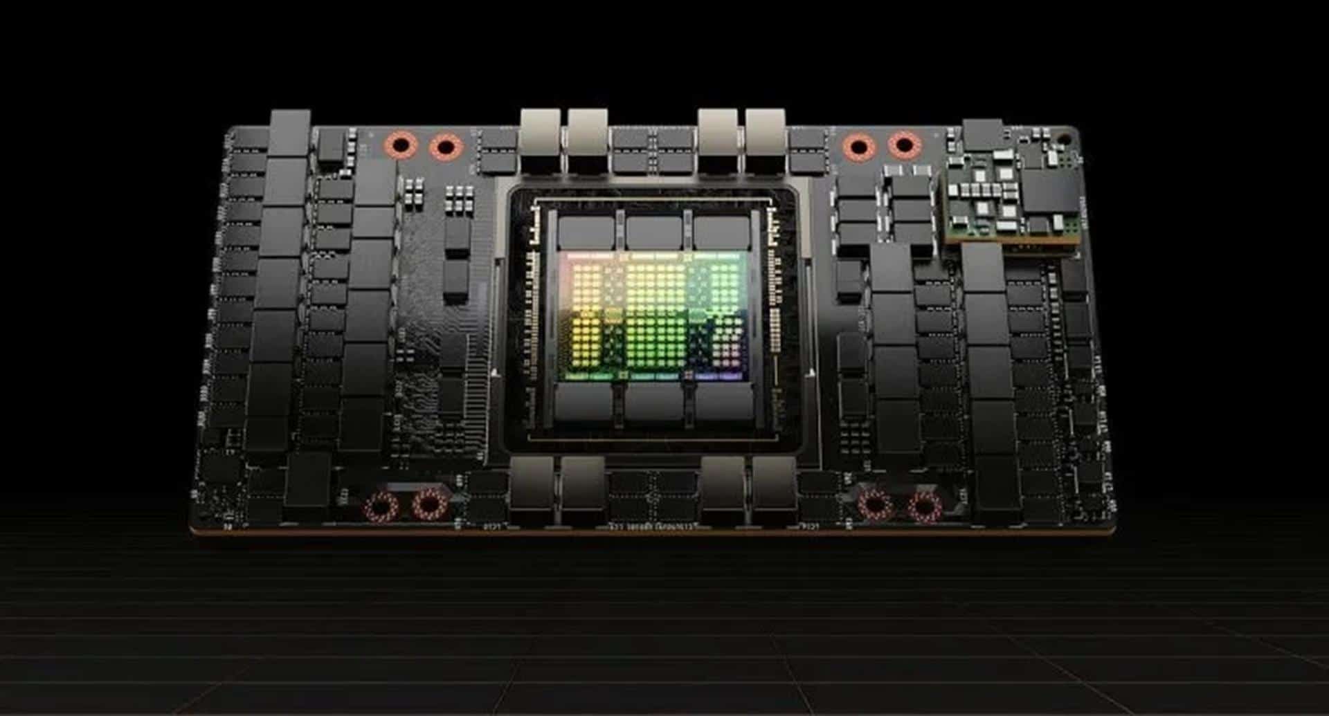
ServeTheHome has published close-up photos that show the most efficient and the latest graphics accelerator in the world in the form of NVIDIA H100 not on PCIe 5.0, but SXM.
The most powerful and newest graphics accelerator finally shown in the picture
The NVIDIA H100 is the successor to the A100, which has a full 80 billion transistors and 16,896 CUDA cores in the SXM version that combine with 80GB of HBM3 memory. The predecessor from 2020 (A100), in turn, offers 54.2 billion transistors, 6912 CUDA cores and 80 GB of HBM2e memory, which clearly shows how much progress NVIDIA has made in the field of accelerators. However, this had a negative effect on power consumption, which jumped from 400 to 700 watts.
Also read: Remember Windows 3D Movie Maker from 1995? Microsoft just reminded about it with an important announcement
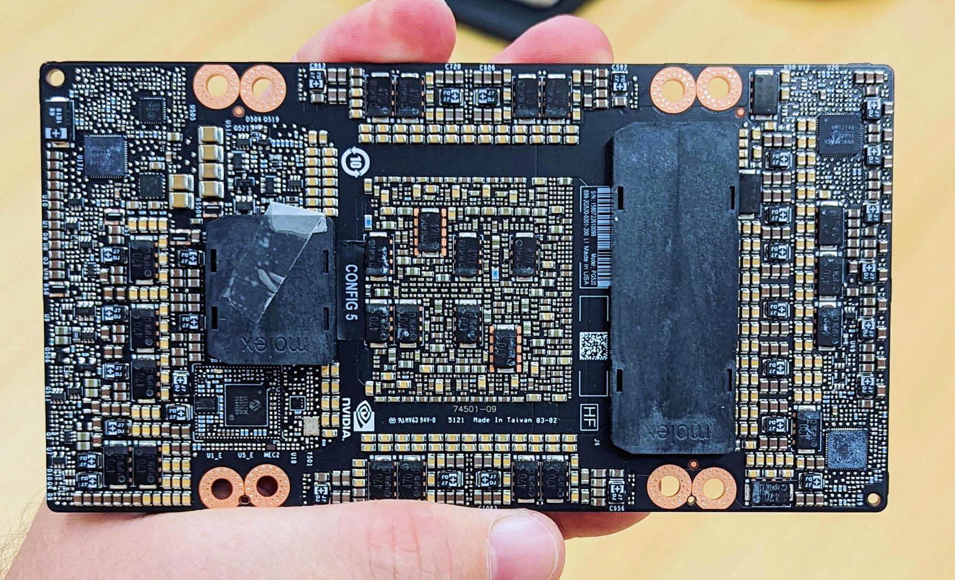
Above, you can see for the first time what NVIDIA has shown us so far only on renderings. It is an 814 square mm graphics processor made in accordance with the 4-nm technological process and Hopper architecture, around which there are a total of six HBM3 memory modules. In addition to the package and the PG520 laminate, there is a whole lot of components responsible for the power supply on the PG520 board.
Related posts:
 The Navi 7nm graphics core is surprisingly efficient
  The paralyzed man starts this year’s World Championships
  This bracelet is the best multitool in the world
  New graphics hidden in AMD drivers
  Raspberry PI 3 has more efficient competition
  ASRock presents a motherboard that supports up to 13 graphics cards