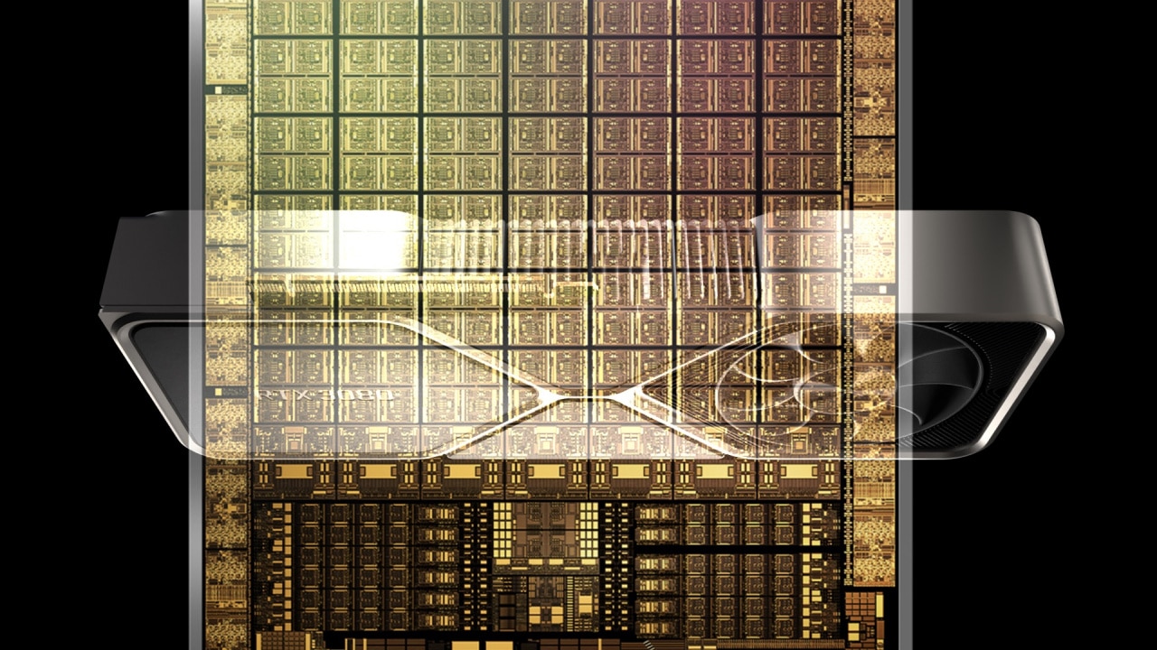
Nvidia’s big premiere party for the architecture Ampere was made with the unveiling of the Geforce RTX 3000 series, which raised eyebrows from time to time with its promising performance shot of mammoth number of CUDA cores. The actual architectural data, on the other hand, was somewhat thin-skinned, something Nvidia is now able to remedy with an insight into the technical changes that Ampere brings “under the hood”.
► Ampere is here – Geforce RTX 3080 doubles the performance of RTX 2080
In addition to the purely architectural changes, Nvidia also illustrates how Ampere differs from both its predecessor Turing and the older architectural sibling Pascal, which kicked off the successful company’s ride since its introduction in 2016. Examples are also given of how traditional raster rendering of CUDA cores performs against the predecessors, the progress of ray tracingperformance and the new possibilities that are added there, as well as a slightly deeper review of the storage technology RTX IO.
Ampere – SM units really swell
Both Ampere and its predecessor Turing mainly share the structure of the circuits’ calculation units (SM), clusters of components that together constitute a complete calculation resource. These components include clusters of CUDA cores, thread handling schedulers (Warp Scheduler), registry files, L1 cache, functional units (FMU), and more.
When the Geforce RTX 3000 series was unveiled, it was not long before the audience was amazed at, and questioned, the abundant number of CUDA cores Nvidia states for all members of the graphics card series. A doubling against the pre-speculation sounded too good to be true, but a review of Nvidia’s technical review shows an approach that in many ways represents a doubling of capacity, even if a SM unit in Ampere does not contain a complete set of everything Turing possesses. .
The CUDA cores in an SM cluster have been expanded to now be able to handle either two floating point calculations (FP32) or an FP32 and an integer calculation (INT32) per clock cycle. An SM unit is equipped with four clusters of 32 CUDA cores, and these can now perform a total of 128 mathematical calculations (FMA), up from 64 for the SM units in Turing. The shared L1 cache also has doubled capacity, it certainly grows by only 33 percent in terms of space, but according to Nvidia’s data, the partitioning between the various CUDA clusters will be twice as large.
Each SM is also equipped with an RT core for calculation of ray tracing and a Tensor core for handling AI and machine learning. The former gets doubled capacity for calculating how light rays intersect (ray intersection) and the latter gets doubled capacity for mathematical calculations of matrices (sparse matrices).
Current ray tracing Nvidia is also going through a new form of ray tracing introduced with Ampere in the form of hardware-accelerated motion blur in RT. When motion blur is to be calculated using conventional RT methods and hardware, calculations are performed on how a triangle is likely to move over time, and then the lighting on the triangles is calculated over time based on this. It is a time-consuming, and thus performance-wise, demanding method for visually advanced games with fast image updating.
With Ampere performed ray tracing-calculations of several triangles, at several times, simultaneously. It generates results for a triangle at multiple time points (samples), which can then be used to create motion blur (output) in ray tracingscenes. According to Nvidia’s data, this provides eight times faster calculations of how rays travel and interact in a scene (ray traversal).
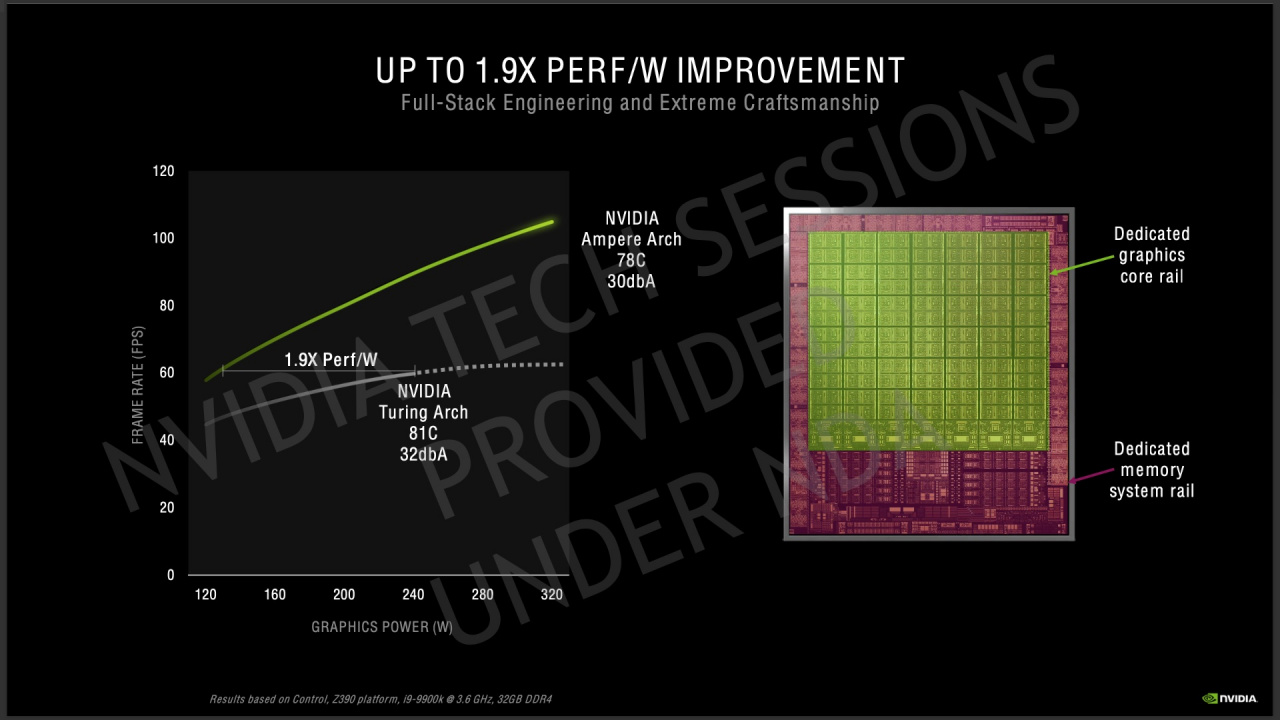
In terms of Tensor cores, the number per SM has actually been halved, from 8 in the Turing circuit TU102 to 4 in the Ampere circuits. Despite this, the total capacity is growing as they are made here by third generation Tensor cores. Where Turing’s SM units can perform 64 FMA calculations of the type FP16 per Tensor core, the Ampere circuit GA102 can perform 128 if it is calculations of sparse matrices (sparse), and 256 if it is large matrices (dense).
A close look at what the SM units in Turing and Ampere can handle, in terms of the total capacity for FMA calculations of the FP16 type, then lands in the same 512 for sparse matrices. For large sparse matrices, on the other hand, the capacity is doubled to 1,024 for Ampere. According to Nvidia’s data, the upgraded Tensor structure provides an improvement of 1.9 × in terms of performance per watt compared to Turing.
With all this in mind, it seems that Nvidia does not embellish the truth too much with what the SM units are capable of in the Geforce RTX 3000 series, even though the components they house in do not grow in step with the number of CUDA cores.
Ampere faced Turing and also Pascal
To further illustrate how Ampere is a big step forward, Nvidia presents the specifications for the new architecture side by side with the equivalent of its predecessor Turing. Here, the Turing generation Geforce RTX 2080 Super is used as the opposite pole to the Ampere and Geforce RTX 3080. Both graphics cards are equipped with six processor clusters (GPC). The number of SM units in RTX 3080 lands at 68, which is not a doubling of the 48 SM units RTX 2080 Super possesses.
Despite this, the number of CUDA cores is stated for the reasons mentioned above to double the number of 8,704 CUDA cores, which reportedly gives a total raster performance of 30 TFLOPS, compared to 11 at RTX 2080 Super. The step in the Tensor Kernels’ floating point calculations becomes even larger, with 238 FP16 DL versus just 89 in RTX 2080 Super. Integrity calculations are also growing impressively with 476 TOPS versus the predecessor’s 178.
The capacity of the GA102 circuit to render pixels on screen and to the graphics memory, measured in gigapixels per second (Gpixels / s), is steadily growing to 164 from 116 in TU102. Current texture rendering, which is measured in gigatexels per second (Gtexels / s), the Ampere circuit achieves a result of 465 Gtexels / s versus the 248 Gtexels / s Turing equivalent. Finally, the memory bandwidth compared to GA102 lands at 760 GB / s, about 25 percent above TU102.
The oh so important latency issue
A cornerstone of how well a graphics card performs is how fast its stream processors can render a frame. To illustrate how Ampere behaves in this respect, Nvidia gives examples of latencies in rendering compared to the results for both Turing and Pascal. In the latter case, results are given for its performance card Geforce GTX 1080 Ti, a for its time very capable circuit without hardware for ray tracing.
According to the example, the GTX 1080 Ti spends about 12 ms rendering a frame with traditional rendering (shading), and if ray tracingcalculations must be performed on its CUDA cores, the rendering time sticks out to 92 ms. When the combination of CUDA, RT and Tensor cores in the Turing architecture is subjected to the same task, the rendering time is reduced to 12 ms. Nvidia also takes the opportunity to compare how Turing performs with shader-based handling of RT, where the time drops from 92 to 51 ms.
When the comparison comes to Turing against Ampere, the newcomer shows impressive results. It is certainly not about a halved rendering time, but neither is it an overly distant result. Where Turing requires 19 ms to render one ray tracingframe Ampere deals with the same frame in 11 ms. When ray tracing combined with the scaling technology DLSS, the time required is 13 ms for Turing while Ampere reaches the finish line of 7.5 ms. When RT and Tensor cores are combined with standard shader units simultaneously, Ampere is ready already at 6.7 ms.
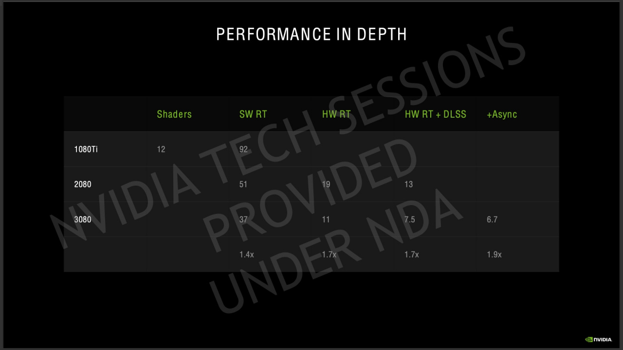
In a concluding overview comparison, Nvidia illustrates how performance has developed over time, from GTX 1080 Ti to RTX 2080 and with a conclusion in RTX 3080. ray tracing calculated in software, Ampere is about 1.4 × faster than the architecture in Turing, and about 3.5 × faster than Pascal. For hardware based ray tracing Ampere is instead 1.7 × faster than Turing, which lacks results for Pascal as it also lacks hardware accelerated ray tracing. When ray tracing and DLSS combined, the progress in the Ampere 1.7 × is set against Turing.
Next generation streamed storage with RTX IO
Microsoft recently lifted the lid on what the Directstorage software interface will lead to significantly improved storage performance for NVME-connected SSD storage as the technology moves to Windows 10 in 2021. The unveiling came just days after Nvidia introduced the related RTX IO technology under Geforce RTX 3000 the event. The two technologies are related and RTX IO will also be compatible with Directstorage when it becomes available.
► Microsoft takes high-performance storage for PC players with Directstorage
In Nvidia’s review of RTX IO, the company gives examples of how retrieving and writing data for both storage and graphics memory, collectively called IO, has changed in recent years and why existing storage interfaces are not designed for modern needs. An example of this is Crysis, which in 2007 took up only 10 GB on players’ hard drives. Today, games often take up sizes of 100 GB, and this is also usually compressed data to be unpacked by the processor.
When storage device calls measure into the tens of thousands, the operating system’s existing storage interface becomes a bottleneck, and new solutions such as Directstorage and RTX IO therefore introduce a new model adapted for streaming large amounts of small data over modern communication interfaces such as NVME. In Nvidia’s example, a hard drive typically delivers 50 to 100 MB / s sustained transfer speeds. For a SATA-connected SSD, this step takes up to 500 MB / s.
With the step over to the NVME interface and the PCI Express 3.0 protocol, the bandwidth grows to 3,500 MB / s, and with PCI Express 4.0 it reaches a full 7,500 MB / s. When today’s software interfaces are to handle these speeds over, for example, PCI Express 4.0, the process of decompressing data between primary memory and graphics memory requires several processor cores. With RTX IO, the decompression is moved from the processor to the cores of the graphics card and is performed there asynchronously to a greater extent than is possible on the processor.
As a concrete performance example, the loading time for a level in a game is stated, partly when uncompressed data is loaded and partly where the processor handles compressed data. Uncompressed data is loaded in 63 seconds, which drops to 38 seconds when the processor unloads. When a test system with the 24-core Ryzen Threadripper 2970WX processor decompresses the data, the time drops to 5 seconds, and when RTX IO is mixed in, it drops to a further 1.5 seconds.
RTX IO will be available in connection with Directstorage taking place in Microsoft’s developer interface DirectX 12, which is planned to take place sometime in 2021, starting with a test version for developers. Nvidia announces that RTX IO can be used with graphics cards from the Turing and Ampere generations, ie Geforce RTX 2000 and RTX 3000 cards.
Summary – not too beautified figures
What Nvidia’s review is gossiping about is that the company’s claims about doubled capacity in the Ampere architecture’s SM units have not been taken off the air. In many of the relevant applications, the Ampere surpasses its predecessor Turing twice, and in cases where this does not happen, the capacity, on paper, is often close to the promised outcome.
We write “on paper” deliberately, because it still remains to be seen how the SM units in Ampere deliver in practice, in different scenarios. In the end, amps are not a duplication of all the components that make up a SM unit, and the different approach is likely to suit different scenarios differently. Whether 8,704 CUDA cores in the RTX 3080 corresponds to the advantage over the RTX 2080 Ti and its 4,352 CUDA cores in practice thus remains to be seen.
Finally, RTX IO in theory seems to be able to bring about the biggest change in storage-related performance gaming fans have seen, perhaps ever. The competitor AMD will probably also provide support for Directstorage in some form in the future. When Microsoft launches Directstorage next year, the spread of the technology should be accelerated, and then players who own an NVME-connected SSD over PCI Express can potentially experience a seven-year lifespan in storage performance.
Read more about “Ampere” and Geforce RTX 3000:
Related posts:
 Review & Test: Video card Gigabyte GeForce RTX 3060 Ti Gaming OC Pro
  AMD Radeon RX 5600 XT VS GTX 1660 Ti and RTX 2060: Review| Set-up| Hashrate
  Review of the KFA2 GeForce RTX 3060 Ti Core video card
  GIGABYTE GeForce RTX 3090 Gaming OC video card: Review| Specs | Set-up|
  INNO3D GeForce RTX 3090 iCHILL X4 video card review: Test | Config | Hashrate
  ROG Strix GeForce RTX 3070 OC Review: Test | Specs | Hashrate