Nvidia Ampere GPU architecture and A100 GPU
: Test |CUP | Specs |Config
tl;dr: Nvidia has revealed the first details of the new Ampere GPU architecture. As the successor to Volta, Ampere’s GA100 is initially aimed at use in the data center for AI training and inferencing. The first ampere GPU A100 is said to be 20 times as fast as Volta in this scenario. The first product is the DGX A100.
First of all, Nvidia Ampere is not for gamers
Nvidia’s new GPU architecture, Ampere, inherits the Volta architecture introduced in 2017 and is thus again a product for the data center – not for gamers. Ampere will also make its way into player PCs, but in a significantly different configuration. It fits that the GA100-GPU (details: Nvidia Ampere: The GA100-GPU analyzed in full configuration) and its first derivative A100 does not support ray tracing – at least Nvidia did not mention this once and the diagram does not show it either.
Nvidia CEO Jensen Huang revealed the first details about the Ampere architecture, the first Ampere GPU A100 and the first products such as the DGX A100 KI system in a recorded GTC keynote today, as the In-house exhibition in San José had to be canceled. A technical deep dive into the new GPU architecture is expected in the course of the coming week.
Nvidia grows with the tasks
Ampere was developed for the exponentially growing resource requirements for training neural networks and inferencing in the data center, explains Nvidia. Compared to previous neural networks such as ResNet-50 for machine vision, which was used when Volta was introduced three years ago, the Megatron-BERT, developed by Nvidia for reading literacy, is 3,000 times more complex.
These new and increasingly complex neural networks enable more and more everyday pervasive applications on the user side, such as AI assistants such as Alexa, the Google Assistant or Siri. But also classic search queries on the Internet, recommendations for online shopping, diagnostics in the medical sector, image recognition or cyber defense are made possible via modern neural networks. These applications support millions of simultaneous requests and have to temporarily provide each user with a small portion of the computing power of the data center for AI acceleration.
Today’s data center is underutilized
According to Nvidia, these trends of increasingly complex neural networks, the increasing number of users and the resulting increase in AI interactions per day have led to fragmented data centers that should be reduced in complexity with Ampere. Currently, data centers consist, for example, of storage servers, CPU servers, AI training servers based on Volta, inferencing servers based on Tesla T4 and servers for general GPU-accelerated tasks, the Volta in a card format that can be installed quickly with PCIe connection. Nvidia argues that the type and quantity of the required computing clusters is difficult for the operator to predict in view of the various applications and the different requirements depending on the time of day, so that optimization for high utilization and cost-efficient operation of the data center is hardly possible.
Ampere should be much faster and more flexible
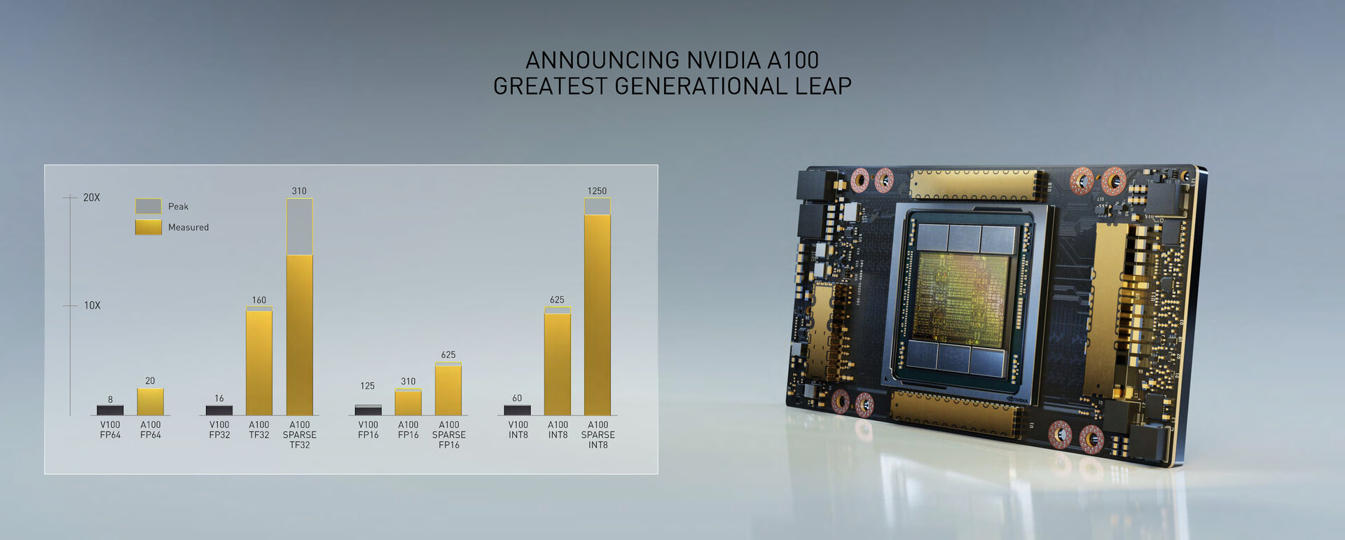
With Ampere, Nvidia not only wants to massively increase performance, but also create a flexible architecture for exchangeable use cases in a dynamic data center that is equipped for a wide variety of modern scenarios. In terms of performance, Nvidia promises under certain conditions a 20 times higher AI performance than with Volta – the biggest leap between two generations of GPU architecture at Nvidia so far. Ampere also combines AI training and inferencing acceleration into one architecture. In terms of scalability, a server can be used as a huge GPU or divided into more than 50 dedicated instances.
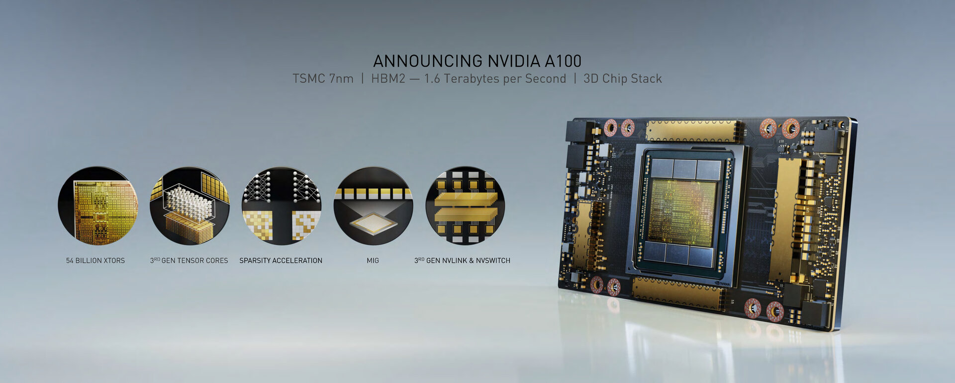
GA100 GPU with 54.2 billion transistors
The first GPU of the new Ampere architecture is the GA100. Like Volta, the GA100 is manufactured by TSMC, but now using the N7 process with immersion lithography (DUV) and has 54.2 billion transistors on an area of 826 mm². With almost the same area (815 mm²) as with the Volta-GPU GV100, that is more than twice as many transistors (21.1 billion). The GV100-GPU is also manufactured by TSMC, but in the 12 nm FFN process. With 54.2 billion transistors on 826 mm², the GA100-GPU is the world’s largest 7-nm chip, according to Nvidia. Each GA100 GPU is supported by 48 GB HBM2 from Samsung with a memory bandwidth of 1.9 TB / s – that’s over 100 percent more than the 900 GB / s from Volta on the GV100. The GPU-to-GPU communication takes place at Ampere via the twice faster NVLink of the 3rd generation with 600 GB / s. More details about the GA100 in the report Nvidia Ampere: The GA100-GPU analyzed in full configuration.
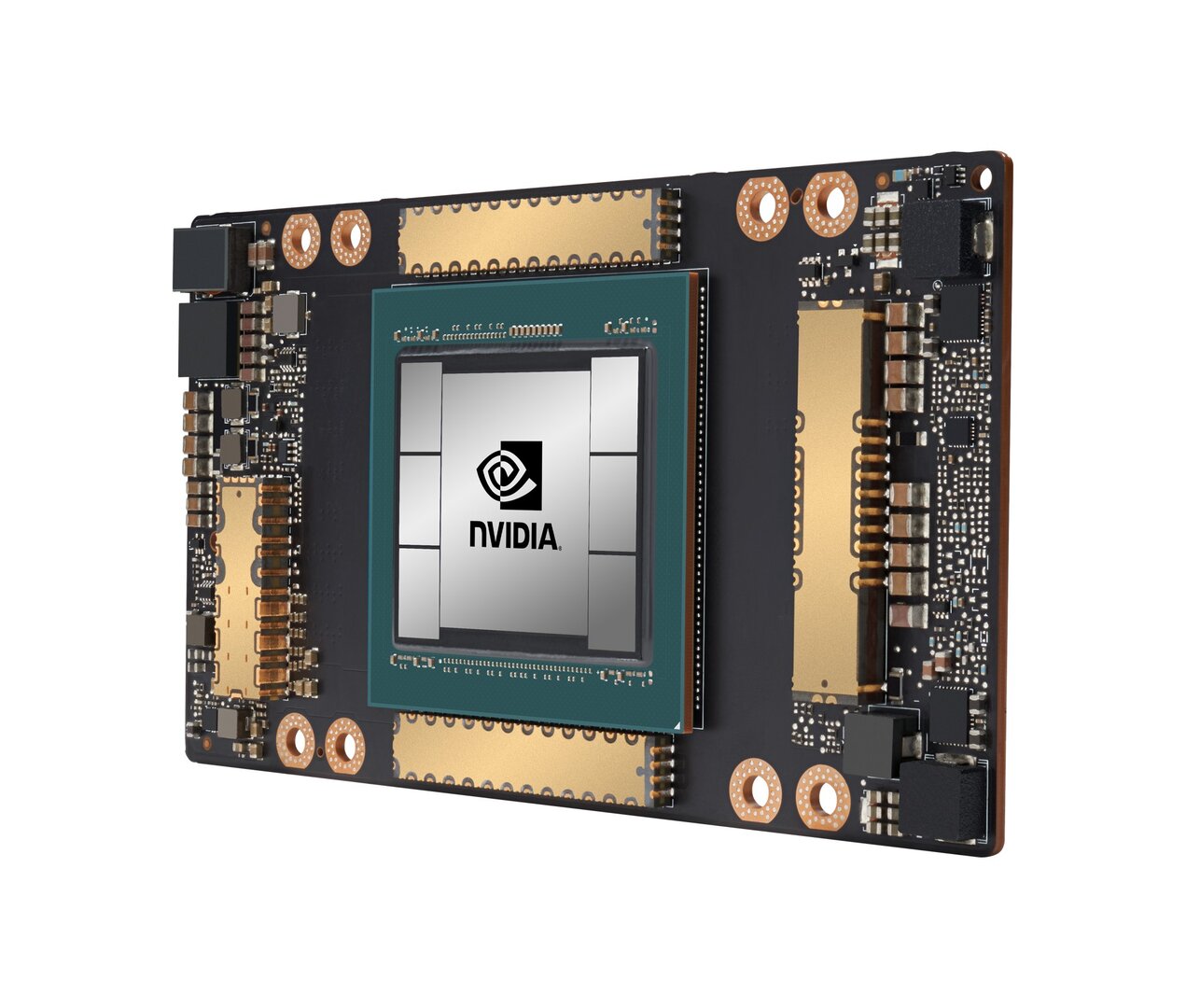
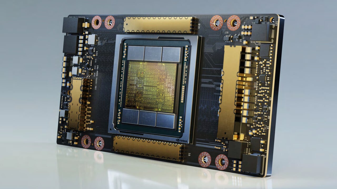
Nvidia A100-GPU (Bild: Nvidia)
image 1 from 2
A100, GA100 and GV100 at a first overview
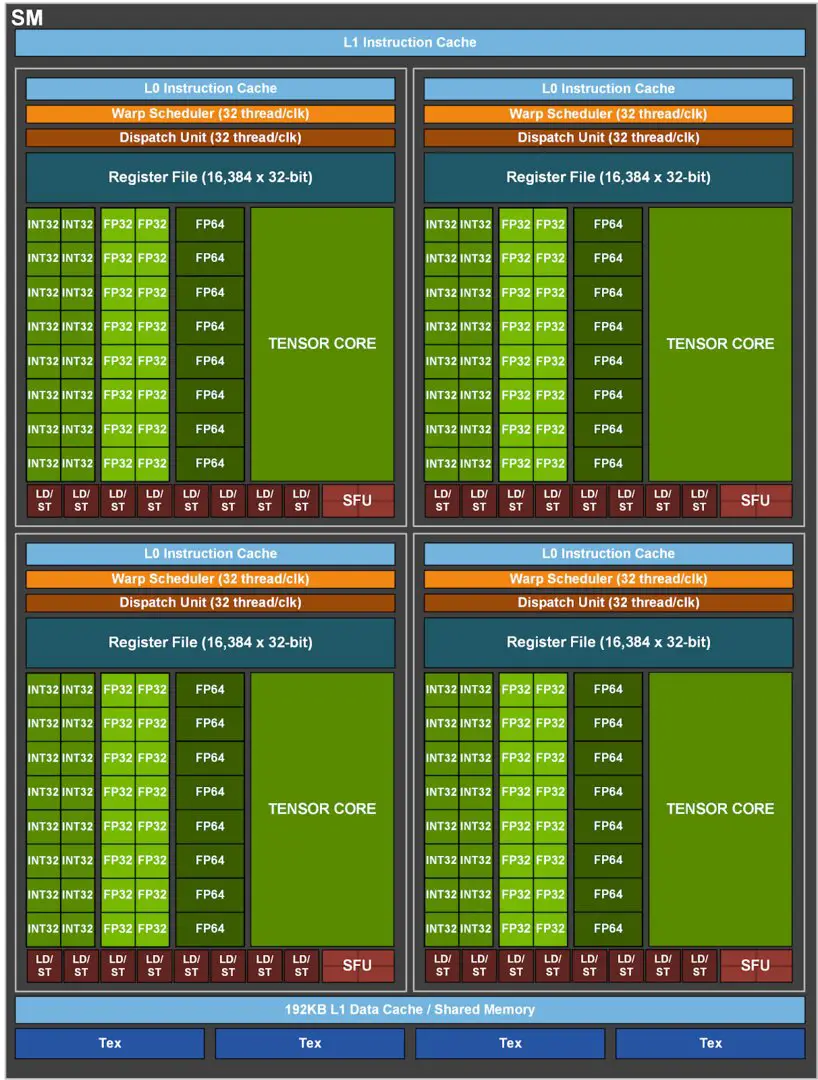
The A100 Tensor Core GPU of the SXM4 module, which is derived from the full expansion GA100 and is significantly trimmed, is equipped with 432 Tensor Cores of the 3rd generation, offers 108 ampere streaming multiprocessors (SMs) and thus 24 more than the full expansion of the GV100 with its Volta -SMs. Each SM of the A100 has 64 FP32-CUDA cores and 32 FP64-CUDA cores.
When Nvidia speaks of a 20 times higher processing power for amps compared to Volta, the company is referring to the tensor cores and their matrix arithmetic operations (MAD) for FP32 and INT8, which are used as standard for AI training and inferencing. The peak computing power of the FP32 is 312 TFLOPS, while the INT8 has 1,248 TOPS – in both cases around 20 times more than the GV100 based on the Volta architecture. For the double-precision MAD FP64, the performance of the tensor cores is 19.5 TFLOPS and thus 2.5 times that of Volta.
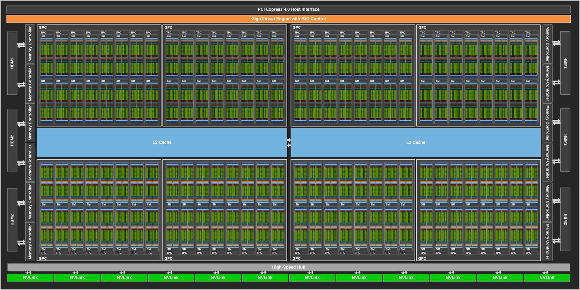
GA100 full expansion with 128 SMs (Image: Nvidia)
image 1 from 2
CUDA cores play a subordinate role
While the AI performance increases massively via the tensor cores and the focus of the architecture seems to be on this area, the classic FP64 and FP32 performance of the CUDA cores grows less dramatically. The peak is 9.7 TFLOPS for FP64 (+ 24 percent) and 19.5 TFLOPS for FP32 (+ 24 percent).
The A100 works at a moderate rate
The clock rate of the A100 can be calculated based on the number of execution units and the theoretical peak performance, even if Nvidia does not officially name any. Accordingly, this is around 1,410 MHz. However, it is still unclear whether the A100 can only work beyond this value for a short time or whether this represents the maximum.
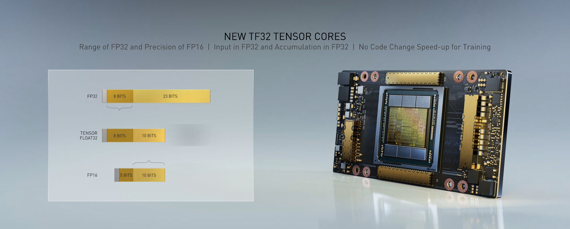
Nvidia calculates FP32 faster over TF32
The 20 times higher computing power is the result of the 3rd generation of tensor cores with new sparsity acceleration – more on that later. The 3rd generation Tensor Cores supports TF32 as a new number format introduced by Nvidia for multiply-add arithmetic operations. With TF32, as with FP32, 8 bits are available for the exponent and, as with FP16, 10 bits are available for the mantissa. With this, Nvidia wants to create a new hybrid format in order to be able to deal with 8-bit variables as in the single-precision FP32 with the 10-bit accuracy of half-precision as in the FP16. At Ampere, TF32 is used as standard for the acceleration of the single-precision FP32 in combination with the new sparsity acceleration. According to Nvidia, developers should still be able to use single-precision FP32 as input and continue to receive single-precision FP32 as output. No changes should have to be made to the code for the new AI acceleration.
New standard MAD TF32 (Image: Nvidia)
image 1 from 2
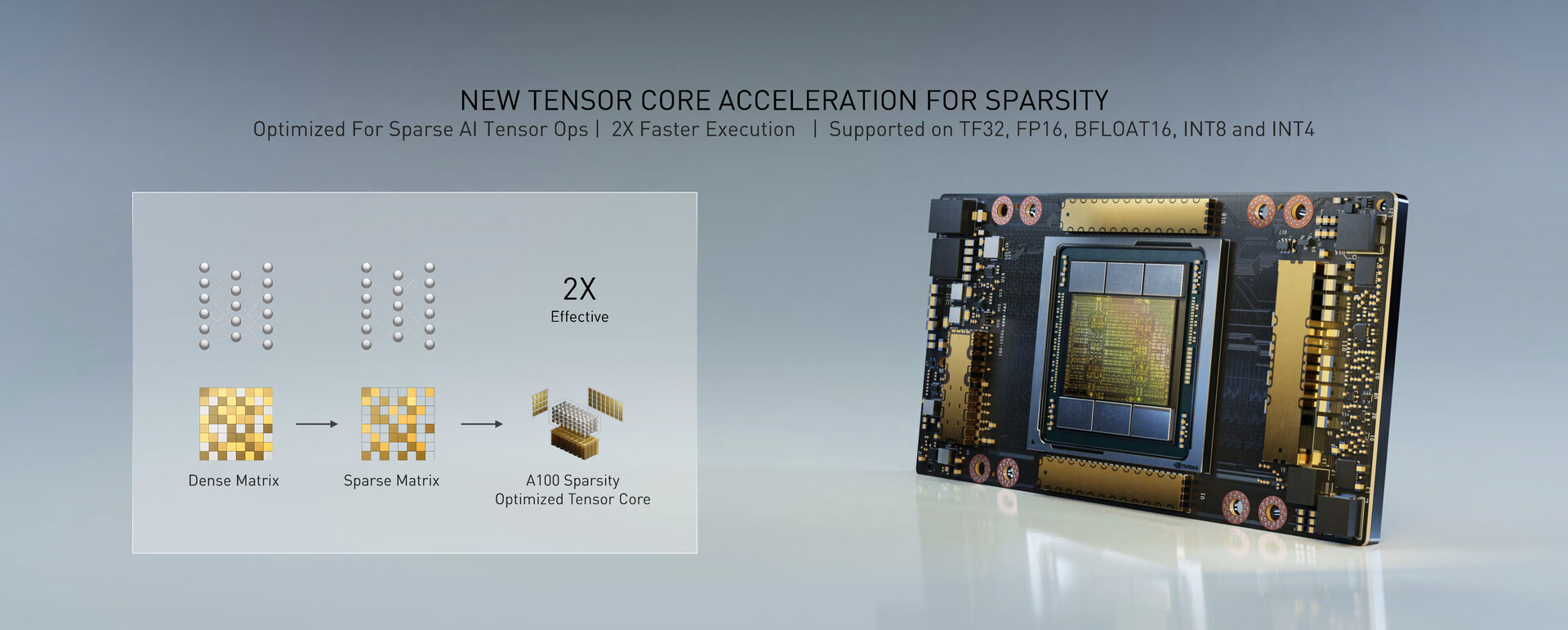
Thin out neural networks
With the sparsity acceleration, Nvidia wants to get rid of the connections of a neural network that are often not required and that do not contribute to the precise prediction. The densely interwoven matrix of the neural network is to be converted into a thinned (sparse) matrix and executed more efficiently and faster. The A100 and its 3rd generation tensor cores have been optimized for this sparsity acceleration, which is used in the TF32, FP16, BFLOAT16, INT8 and INT4.
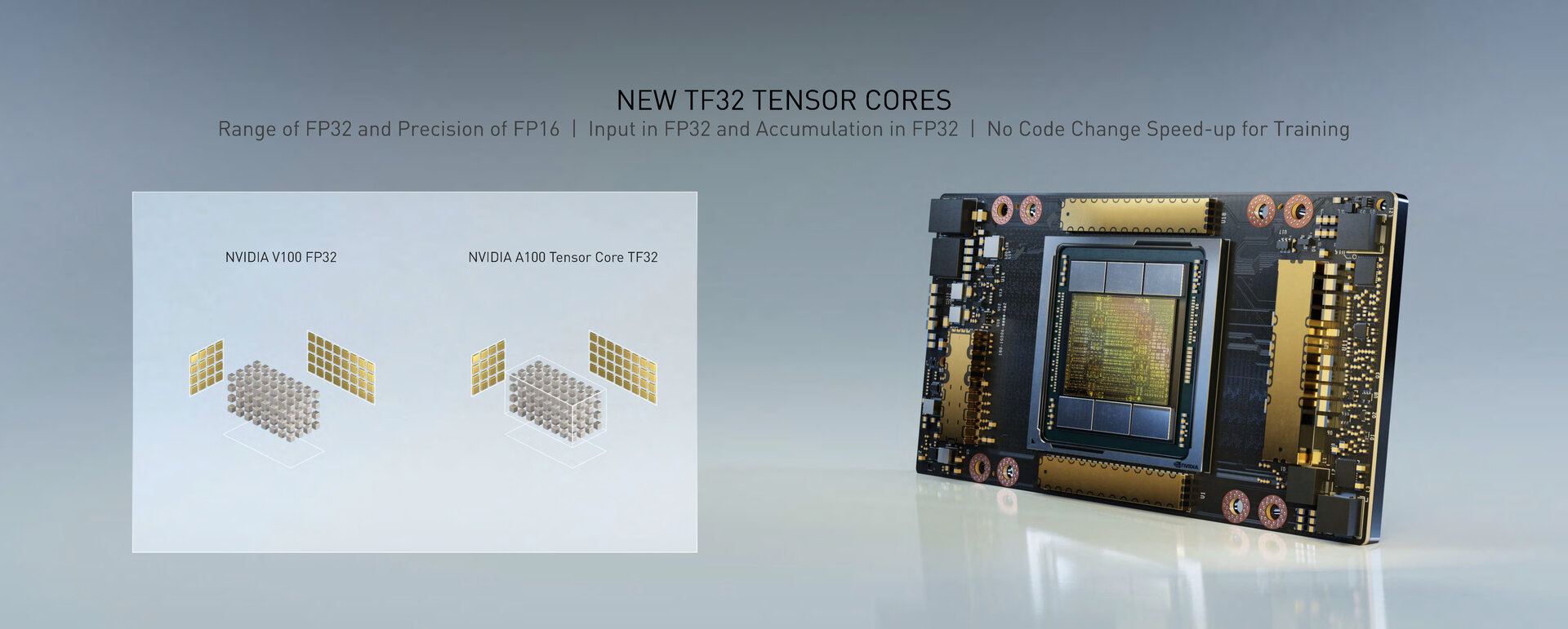
This in turn explains the immense leap in performance for the FP32 and INT8 at Ampere, which is only available when the new number format TF32 or the sparsity acceleration are used. 16 TFLOPS for FP32 on the GV100-GPU become 160 TFLOPS for TF32 (as the new standard for FP32 operations) on the A100-GPU. And with sparsity acceleration, it then becomes the propagated 20 times higher 312 TFLOPS with spare TF32. The same applies to INT8 operations in inferencing, which grows from 60 TOPS for GV100 to 625 TOPS for A100 and finally 1,248 TOPS for A100 with Sparse INT8. Since the new acceleration does not apply to Double-Precision FP64, this also explains the comparatively smaller jump by a factor of 2.5 to 19.5 TFLOPS. It also explains why the A100 with only 432 instead of 672 tensor cores with the GV100 is still much faster.
Probably 5 HBM2 stacks and a dummy
If you look at the picture of the A100, you will see six HBM2 stacks. It is surprising how the hardware should have 40 GB of memory, with six stacks that would not be possible without further ado. Nvidia has not yet commented on this – that will only happen in the course of next week – but apparently the A100 does not have 6 HBM2 stacks, but only 5 and a dummy stack to compensate for the contact pressure of the cooler. With 5 stacks and 8 GB per stack, you get 40 GB of memory. The memory interface would thus be 5,120 bits wide (1,024 bits per stack), so that the HBM2 memory would have to work at 1,250 MHz to achieve 1.6 TB / s.
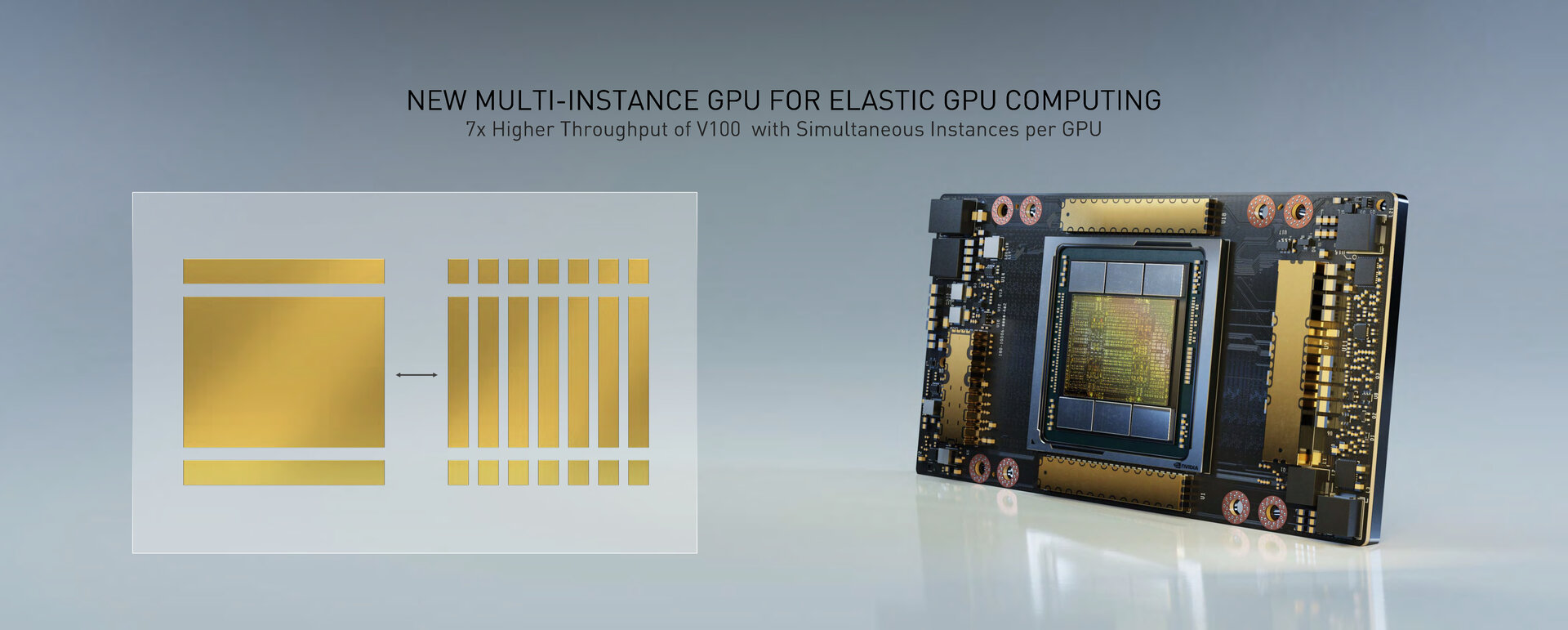
7 dedicated GPUs on one A100
In addition, Multi-Instance GPU (MIG) is one of the major innovations in the Ampere architecture. Each A100 can be divided into up to seven dedicated GPUs, as not every application requires the full performance of the entire GPU. The fact that several instances can run on one GPU is not new to Nvidia per se, and this is also possible with Volta, but Ampere is introducing for the first time that each of these GPUs is assigned dedicated hardware resources. According to Nvidia, each instance has its own tensor and CUDA cores, its own cache, its own HBM2 and its own memory bandwidth, which should prevent interference between the individual GPUs or applications running out of resources. From the point of view of the application, each GPU instance should act like an independent GPU.
NVLink works at 600 GB / s
While an A100 GPU can be divided into up to seven GPUs, this also works in the opposite direction and several GPUs in several servers can be linked to form a large computing cluster. So that there is no bottleneck during this process, Nvidia has doubled GPU-to-GPU communication with a new generation of NVLink from 300 GB / s to 600 GB / s. Using the NVSwitch as a switch for multiple NVLinks, a bidirectional bandwidth of up to 4.8 TB / s is available, as required in the first product with an A100 GPU, the Nvidia DGX A100.
On the next page: DGX A100 comes with eight A100 GPUs
Related posts:
 7-nanometer Nvidia GPU, TSMC will handle most of the production
  ASRock X299, a new BIOS allows you to install 2 TB of memory
  MSI Prestige X570 Creation Review: Test | Specs | Hashrate
  Radeon RX 5500 XT, PCI Express 3.0 castrates performance?
  An overclocker ran 1TB of RAM on an X299 motherboard limited to 256GB
  Best Review 2021: MSI MPG X570 Gaming Edge WiFi Under $250 ($200)