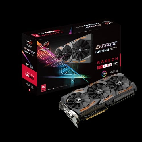
AMD Radeon RX 480 8GB Review | Get to know Polaris 10
Eight months ago, AMD began unleashing the power of the next generation of GPUs, starting with an updated display controller that supports HDMI 2.0b, DisplayPort 1.3 HBR3, FreeSync over HDMI, and an HDR-compatible pipeline. Later, additional information began to appear, which talked about the release of two different GPUs, one of which was designed specifically for the mainstream desktop market, and the other for mobile solutions that offer console-level performance in thin and light form factors.
The second product includes 16 computing units (CU), 128-bit memory bus, and accelerated 4K video encoding/decoding. It’s not yet available. The AMD Radeon RX 480 video card uses a larger Polaris 10 processor design. In terms of physical size, it’s no bigger than the Nvidia GP100 processor with 15.3 billion transistors, but it’s enough to handle the best virtual reality headsets. In terms of performance, the card is on par with the AMD Radeon R9290 and Nvidia GeForce GTX 970.
The card’s mid-range performance barely catches the eye, especially when compared to the new Nvidia GP104 GPU. However AMD Radeon RX 480 its cost is much lower than similar solutions in speed, and power consumption is limited to 150 watts. Thus, AMD expects to make virtual reality available to a wider audience of gamers (it would be nice to play companies selling HMDs for $800 and $600).
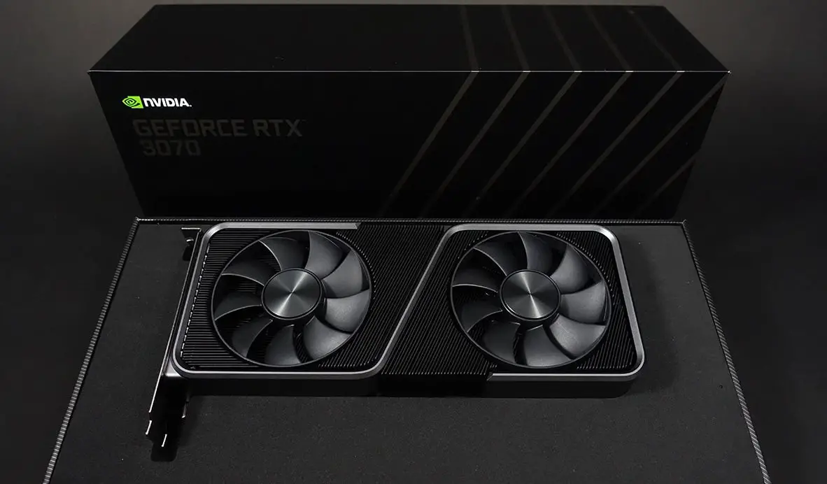
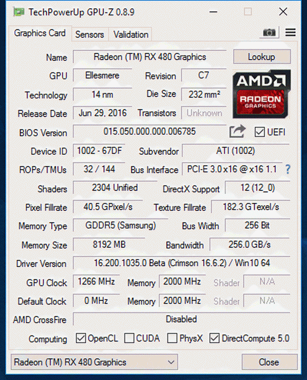
Two versions available AMD Radeon RX 480 : $200 (MSRP) model with 4GB GDDR5 7Gbps video memory and $240 (MSRP) version with 8GB GDDR5 8Gbps video memory. Today we are testing the 8GB model.
Features of Polaris 10
The Polaris 10 consists of 5.7 billion transistors on a 230 mm 2 chip. By comparison, a Hawaiian crystal contains 6.2 billion transistors and has an area of 438 mm 2. Despite having fewer transistors and 55% lower power consumption, the RX 480 falls between R9290 and 390 in most tests. This is largely due to GlobalFoundries’ 14nm FinFET process, which gives AMD superior performance and power advantages over AMD. Planar transistors are manufactured using 28nm process technology. FinFET delivers a higher frequency at any power consumption level, and vice versa, at any clock frequency, as a 14nm chip consumes less power. In the case of Polaris, AMD took advantage of both by increasing clock speeds and lowering power consumption. So it was able to outperform the more powerful Hawaii GPU while maintaining a power ceiling of 150W (although our measurements show that number is a bit understated).
Despite the new codename, the Polaris 10 is based on the fourth generation of the AMD Graphics Core Next architecture. Therefore, the basic building blocks of the Polaris processor design will seem familiar to many enthusiasts, and it will be easier for us to describe them.
Specifications
| AMD Radeon RX 480 | AMD Radeon R9 390 | AMD Radio R9290 | |
| Polaris 10 | Grenada Pro | Hawaii Pro | |
| computing units (CU) | 36 | 40 | 40 |
| stream processors | 2304 | 2560 | 2560 |
| Clock frequency (base / boost), MHz | 1120/1266 | 1000 | 947 |
| Peak calculation rate, GFLOPs (at fundamental frequency) | 5161 | 5120 | 4849 |
| number of fabric blocks | 144 | 160 | 160 |
| Texture Fill Acceleration Gtex/s | 182,3 | 160 | 160 |
| Number of Royal Oman Police units | 32 | 64 | 64 |
| L2 cache size, MB | 2 | 1 | 1 |
| Memory data transfer rate, GB/sec | 8 (8 GB) / 7 (4 GB) | 6 | 5 |
| Memory bandwidth, GB/sec | 256 | 384 | 320 |
| Memory bus, bit | 256 | 512 | 512 |
| Thermal packaging, W | 150 | 275 | 250 |
| Number of transistors, billion | 5,7 | 6,2 | 6,2 |
| Crystal area, mm 2 | 230 | 438 | 438 |
| Technological process, nanometer | 14 | 28 | 28 |
| Initial price | $240 (8 GB) / $ 200 (4 GB) | $330 (8 GB) | $400 (4 GB) |
One GCP-Graphics command processor is still responsible for sending the sequence of graphics instructions to the Shader Engine. Asynchronous Computing Engine (ACE) takes care of the arithmetic instruction sequence. Instead of just eight ACEs, the command execution logic now consists of four ACEs and two hardware schedulers, which perform the tasks of prioritizing queues, managing time/spatial resources, and offloading scheduling tasks to the CPU kernel mode driver. In essence, these are not separate or new blocks, but an additional way in which existing pipelines can operate. Dave Nalasco, Senior Director of Graphics Workflow Operations at AMD commented:
HWS (Hardware Workgroup/Wavefront Schedulers) are basically ACE pipelines without transmission controllers. Their job is to offload the CPU by controlling the scheduling process for user/driver defined queues on available hardware queue slots These are small code programmable processors that can implement different scheduling policies. We used them to implement QR queuing and CU reservations. We were also able to pass these changes to GCN 3rd generation graphics cards through driver updates.”
Rapid Response Queuing allows developers to prioritize specific tasks that run asynchronously without completely preempting other processes. A more detailed explanation can be found on Dave’s blog (English). In short, AMD wants flexibility. Its architecture allows for different approaches to optimize resource usage and reduce display latency, both of which are important for virtual reality applications.
Known computational CUs consist of 64 shaders, compliant with the IEEE 754-2008 standard, divided into four vector units, a standard unit, and 16 load/storage units for a texture sample. In addition, each controller includes four synthesis units, a 16KB L1 cache, 64KB of local space for data exchange, and a logging space for vector and scalar units. AMD claims to have made several tweaks to improve CU efficiency, including adding support for FP16 (and Int16), improving cache access, and improving the appearance of instructions. Together, these changes provide up to 15% better CU performance compared to Hawaiian (2nd generation GCN) GPUs.
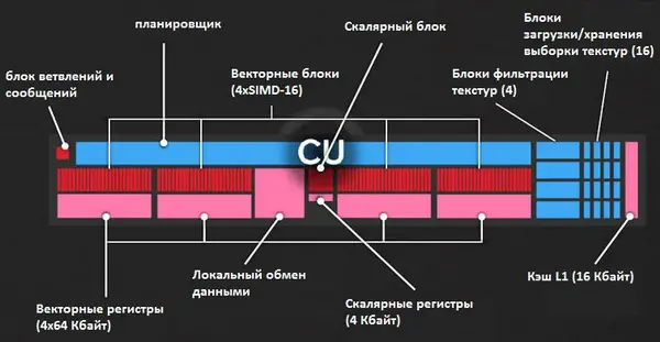
Nine working units make up a large shader unit (SE – Shader Engine). The Polaris 10 video chip has four of these layouts and we know that’s the limit for this architecture. A total of 2,304 stream processors and 144 mounting units (64 shaders × 9 CU × 4 SE) were obtained.
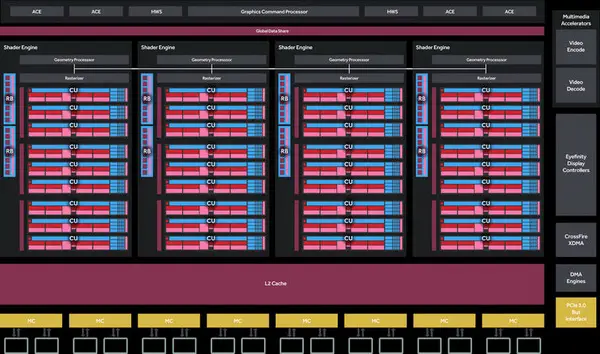
Each shader unit is associated with an engineering engine (GE) unit. According to AMD, a primitive discard accelerator has been added to the engineering block, which filters out even the simplest geometric elements that have not been pixelated before scanning the transformation, thereby increasing productivity. This is an automatic pre-rasterizing feature for the graphics pipeline and is new in Polaris. In addition, an index cache of cloned geometry appeared, although we do not know its size and degree of influence during cloning.
By analogy with a Hawaiian video chip, the Polaris 10 processor is capable of delivering four simple elements per cycle. However, compared to Hawaii/Greenada GPUs up to 1050MHz (in the case of the R9 390X), AMD bumped the base clock of the AMD Radeon RX 480 up to 1120MHz, and the boost-mode frequency up to 1266MHz. It turns out that the company compensates for the loss of resources on the crystal with an increased frequency. The Radeon R9290X’s single-resolution floating point performance is 5.6 TFLOPS, while the RX 480 reaches 5.8 TFLOPS in Boost mode.
How realistic is the clock speed of 1266MHz? The Hawaii GPU had a hard time keeping up with the specs because it got too hot, and we wanted to make sure that didn’t happen with Polaris. Using GPU-Z, we measured the clock speed in the integrated benchmark of Metro: Last Light Redux, iterated 10 times in a row, and received the following graph:
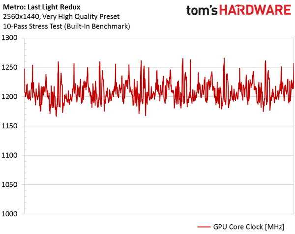
Stress Test Clock – Built-in Metro: Last Light Return Scale, 10 Passes, MHz
The difference between the high (1265MHz) and bottom (1118MHz) points on the graph is 148MHz. We can say that AMD fits well within the indicated limits, despite constantly adjusting the frequency during testing. But the average u200bu200b1208MHz is at least closer to the top.
Both the Hawaii and Fiji SE GPUs have four wallpapers capable of outputting 16 pixels per hour (64 pixels per hour in total). Polaris 10 cut this component in half. Each SE has two display backlights, each with four ROPs, offering 32 pixels per hour in total. The difference with the Hawaii-based Radeon R9290 is significant. The situation is aggravated by the 256-bit Polaris 10 memory bus, which is twice the size of the memory bus for the Hawaiian (512-bit) video chip. The AMD Radeon RX 480 uses 4GB of GDDR5 at 7Gbps and has a throughput of 224GB/s, while the 8GB model we’re testing today uses 8GB/s of memory and bandwidth up to 256GB/s. But in any case, this is much less than the 320 GB / in the R9290.
The decrease in hardware resources is partially offset by improved delta color compression, which reduces the amount of information transmitted over the bus. AMD also supports lossless 2/4/8:1 compression, just like the Nvidia Pascal architecture. Additionally, Polaris 10 uses a 2MB cache, the same size as Fiji. This will reduce the number of GDDR5 memory accesses and reduce the GPU’s dependence on a broad bus and high bandwidth.
However, exhausting the GPU backend should affect performance with increased fineness and intensity of anti-aliasing. We wondered what Polaris would look like against Hawaii with increased intensity. To test this, we ran a benchmark Grand Theft Auto V at a modest 1920 x 1080 resolution with “very high” graphics detail settings and gradually increased the anti-aliasing quality.
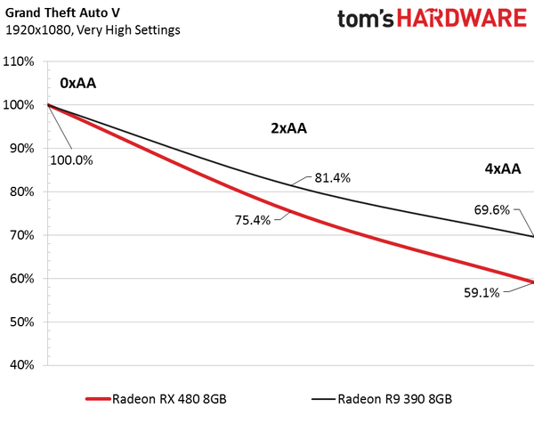
The graph clearly shows that when changing MSAA anti-aliasing from 2x to 4x the AMD Radeon RX 480 loses the average frame rate u200bu200 much faster than the R9 390. With anti-aliasing disabled, the RX 480 reaches 97.3 fps and the R9 390 – 90.4 fps. But towards the end of the table the AMD Radeon RX 480 showed only 57.5 fps, while the u200bu200b390 averaged 62.9 fps.