– In the future, chip production will no longer be possible without EUV lithography. BitcoinMinersHashrate explains what lies behind the new evolution in exposure technology and looks back at the hurdles that had to be overcome from theory to practical use.
Excursus: How are chips made?
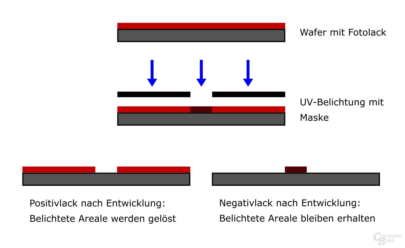
Nowadays, semiconductor chips are manufactured exclusively by means of photo-lithography. Photoresists are exposed on wafers and the resulting structures are then transferred to the silicon of the wafer. BitcoinMinersHashrate reported this process some time ago in the report From Silicon to Die: Chips from wafers in the clean room are described comprehensively using a practical example.
Extreme UV lithography
The exposure of semiconductor chips with extreme ultraviolet radiation (Extreme UV or EUV) will be in the foreground in the future when manufacturing new processors and graphics cards. It has been talked about for years, now it is slowly getting ready for the market. The basis for the following elaborations is that in the summer of 2019 in the magazine Journal of Microelectronic Manufacturing published scientific articles
EUV Lithography: State-of-the-Art Review by researchers from HiSilicon Technologies, a Huawei subsidiary.
That is behind the exposure
Semiconductor exposure to light and other electromagnetic radiation is essential for the production of silicon-based chips, such as those used in processors, graphics cards, microcontrollers and SoCs. A key feature of increasing performance and falling manufacturing costs is the progressive reduction in the size of structures in production, which enables ever more performance in an ever smaller space. The wavelength of the selected exposure source plays a central role in this reduction, because smaller wavelengths enable smaller, minimally exposed structures.
The reason for this is the Abbe limit, a fundamental limit for the smallest point on which light can be focused using a lens. The Abbe limit is proportional to the wavelength of the light and anti-proportional to the refractive index of the medium. This means: Shorter wavelengths and higher refractive indices enable smaller structures.
While the so-called G-line with 436 nm wavelength was still used in the 1970s, the development ended with the introduction of deep UV (DUV) and 193 nm wavelength in 2001. immersion lithography, in which wafers and the exposure optics are immersed in water. The higher refractive index of water (1.44) compared to air (1.00) made it possible to further reduce the structure sizes. The combination of immersion lithography and DUV brought about the progress of production up to the current 10nm / 7nm FinFET node from Intel and TSMC.
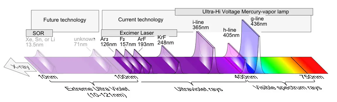
After years of delay, the next exposure stage with a wavelength of only 13.5 nm is now mass-producing, which should be the basis for all future manufacturing technologies: EUV.
The upcoming AMD products based on Zen 3 and RDNA2 will not only herald the arrival of EUV products for millions of consumers. Samsung has had several chips with 7 nm EUV on the mass market since last August, and Huawei's high-end chips also use TSMC's EUV production.
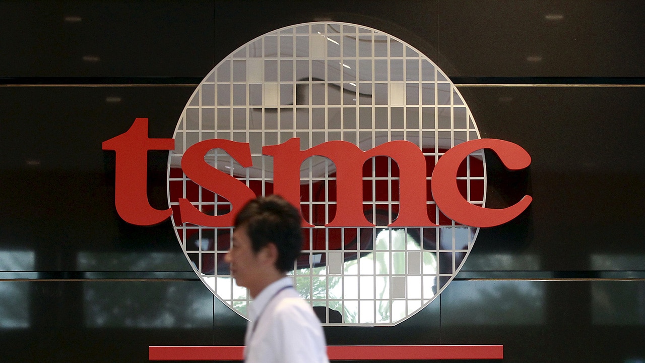
The basis for the production with EUV lithography is always the Dutch company ASML, which initially exclusively produces the exposure machines and has the difficult task of converting the findings from academic research into tangible components. The value of the ASLM share has almost tripled in the past five years.
Ten years from theory to practice
But what hurdles were overcome when moving to the EUV? What were the challenges? And how much breathtaking technology is in the current manufacturing systems?
The light source
Originally, individual spectral lines of the mercury lamp were selected for exposure in lithography. In contrast, argon fluoride lasers have been used to generate DUV with a wavelength of 193 nm since the 2000s. The search for a suitable, stimulable laser medium is the challenge when exposing with ever shorter wavelengths.
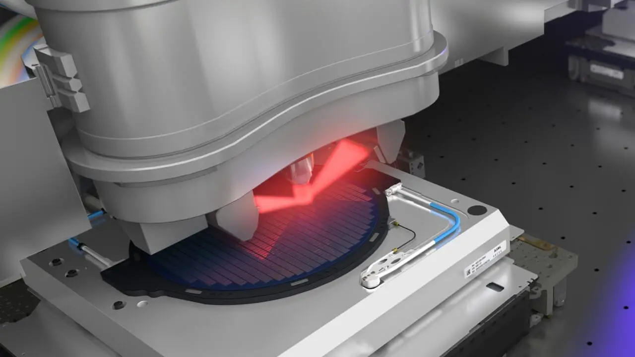
The generation of radiation with a wavelength of only 13.5 nm places immense demands on the technology used in the light source. The light is obtained from a plasma made of tin, which is excited using a short pulse laser. In order to generate the plasma, the 20 outer electrons must first be removed from each atom of a microscopic tin droplet. Twenty times positively charged Sn20 + ions are formed. The 21st electron is then excited with the help of a high-performance CO2 laser with 40 to 60 kW and generates the desired high-energy radiation when it falls back into atomic orbit, similar to the flame coloring of fireworks. The duration of the laser pulse is only 10 ns. Efficiency is only six percent: the ASML NXE: 3400B uses a 40 kW laser to obtain 250 W EUV radiation, which enables the exposure of 140 wafers per hour. The ASML NXE: 3400C, which has been manufactured since July, is already a further development.
The 27 µm droplets of molten tin have to be dripped into the chamber with the same size and at regular intervals so that the process is stable. The procedure is also described as an angry bird process, since you have to ignite the laser at the right moment to optimally hit the tin droplets.
Since the positively charged and laser-bombarded Sn20 + ions repel each other, there is a risk of tin deposits in the otherwise highly pure and under-pressurized chamber. These contaminants were one of the greatest challenges in the development of EUV systems. ASML solves this by introducing hydrogen into the chamber at very low pressure, which reacts with the tin to form tin hydride and can be pumped out.
Now the light is generated, but far from where it is needed for the exposure.
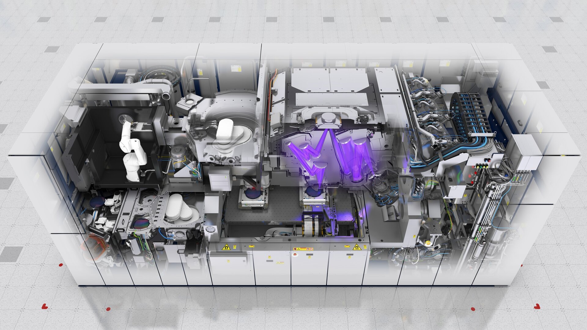
Reflection system and optics
Transparent optics cannot be used for EUV due to their high absorption in the UV range. Instead, reflective optics have to be used. Shielding gases also absorb too much radiation, which is why the entire beam path must be enclosed in a high vacuum system. Both properties clearly distinguish an EUV lithography system from the previously used DUV systems, which is why suitable components had to be completely redeveloped.
Conventional mirrors made of silver or aluminum are not suitable for use with EUV due to their very high losses. Instead, Bragg mirrors made of alternating layers of molybdenum and silicon are used. At 70 percent, these are sufficiently reflective for 13.5 nm and can also filter out undesired wavelengths.
Like the other components, they have to be manufactured with high precision and have to be high-purity layers with an exact thickness and extremely smooth polished surface in order to avoid losses. The combination of molybdenum and silicon also prevents premature aging and oxidation due to EUV radiation. The evenness of the coating now has a variation of less than 0.5 percent over a complete 150 mm wafer. ASML works here with Zeiss.
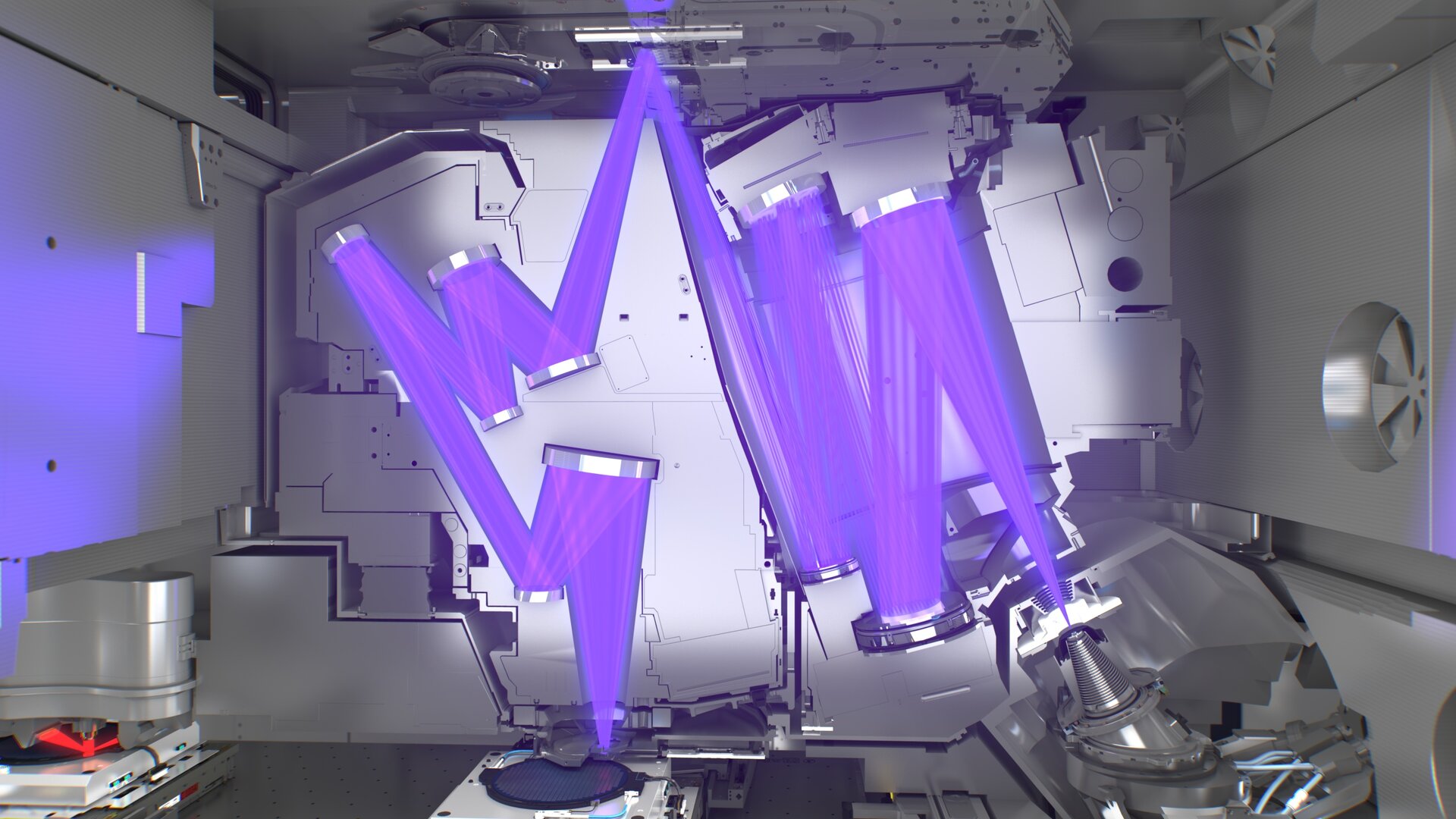
For the reasons mentioned above, the focusing optics also consist of reflectors, which again necessitated a new development. Accordingly, the first systems have a relatively low focusing strength, expressed by the numerical aperture (NA) of NA = 0.33, which corresponds to an angle of incidence of approximately 20 °. Established DUV optics achieve a NA of almost 1 through an angle of incidence close to 90 °, with immersion lithography the NA increases to up to 1.33. Advances in future manufacturing steps such as 5 nm will benefit significantly from increases in NA. Improved optics with NA> 0.5 are currently in development and, in addition to a significant increase in the mirror area, also require the switch from spherical to aspherical focusing mirrors.
EUV masks
Photomasks shade the areas of the wafer that are not to be exposed and thus define the structures produced. This is conventionally done using the transmission method, which means that areas that are not shaded let the light through the mask. The photo masks for EUV lithography represent a special challenge, since EUV is absorbed by a large number of materials and converted into heat. So that the material does not heat up and burn, the mask must reflect. Conversely, this means that each mask is a Bragg mirror for every intermediate step. The shading is achieved by absorbers made of tantalum nitride. A layer of ruthenium serves as an infrared emitter to radiate the heat generated in the absorbers.
Since the beam path is extremely sensitive to contamination, protective screens are placed in front of the mask, which close off the beam path from the outside. Since these panes can absorb the EUV radiation again, the application is a compromise to ensure the purity in the beam path. Silicon nitride is a promising material with low absorption, which in some research approaches is combined with graphite, graphenes or carbon nanotubes to enable optimal dust protection with minimal thickness.
Another challenge in recent years has been to make the substrate of the mask after a study showed that 75 percent of the defects occurred from substrate manufacture and only 25 percent from the subsequent deposition of the Bragg mirror and the mask coating. By optimizing the manufacturing specifically for EUV substrates, mask manufacturing, which is usually the responsibility of supplier companies such as Applied Materials, has been brought so far in the past two years that roughness, deformation and other defects are low enough to be used commercially.
EUV masks are much more susceptible to contamination in each of the many layers. Since the mask is used in reflection, the smallest changes in the materials produce phase differences in the reflected light, which become visible on the wafer as a so-called speckle. The effect is similar to the pattern you get when you point a laser pointer at a supposedly smooth wall. The smaller the wavelength used, the smaller the phase differences must be before they destroy the desired lithography pattern. Since these phase differences are also invisible to a scanning electron microscope, the EUV masks must instead be inspected with EUV light (actinic inspection), which further increases the cost of the corresponding measurement technology. In some cases, contaminants can be removed with an electron beam after inspection, which saves the mask.
EUV photoresist
The last component for the successful exposure of a wafer is the photoresist, which is designed as a positive or negative lacquer depending on the material. After exposure, the exposed or unexposed part of the photoresist, corresponding to a positive or negative photoresist, is removed using a developer. First of all, the sensitivity of the lacquer for exposure to the corresponding wavelength of 13.5 nm is important. As soon as a suitable material is found, an attempt is made to bring the development process to the desired result with varying developers, development times, lacquer thicknesses and radiation doses. There is always a compromise between the achievable resolution, the sensitivity of the photoresist and the line roughness. For EUV, countless materials with all of these possible combinations were examined experimentally, sometimes with numerical simulations, before commercial solutions could be demonstrated.
A special feature of EUV is the high energy of the individual photons, which often excite more than one electron in the photoresist and can cause chain reactions, which significantly increases the roughness of the individual structures compared to DUV. The recipes for photoresist development had to be painstakingly adapted to what reduced the critical line roughness to currently 3.5 nm. In addition, photoresists can outgas during the exposure, which entails additional protective devices for maintaining the negative pressure in the beam path.
Conclusion
There is no denying that EUV can finally be used in the mass production of semiconductor wafers and expectations are high. But how difficult it was to get here can only be seen by looking back at the hurdles that international cooperation in research and development could achieve. According to its own information, ASML started work on a prototype in 2001, which finally appeared in 2006. Ten years ago, the first prominent delivery of an EUV system to TSMC took place.
It will be seen in the next few years whether all of this will bear fruit and the reduction in structure sizes will continue as usual. The first products from EUV production for the home PC will probably be available in the second half of this year.
This article was interesting, helpful, or both? The editors appreciate any support in the form of deactivated ad blockers or a subscription to BitcoinMinersHashrate. More on the topic of advertisements on BitcoinMinersHashrate.
Related posts:
 7-nanometer Nvidia GPU, TSMC will handle most of the production
  ASRock X299, a new BIOS allows you to install 2 TB of memory
  MSI Prestige X570 Creation Review: Test | Specs | Hashrate
  Radeon RX 5500 XT, PCI Express 3.0 castrates performance?
  An overclocker ran 1TB of RAM on an X299 motherboard limited to 256GB
  Best Review 2021: MSI MPG X570 Gaming Edge WiFi Under $250 ($200)