Xe HPC and Ponte Vecchio, Intel wants to oust AMD and Nvidia from supercomputers
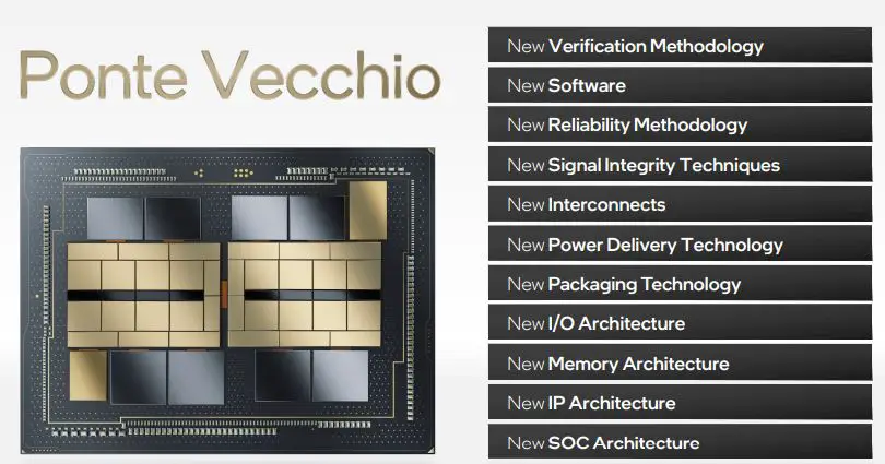
Not only Xe HPG, but during the Architecture Day 2021 Intel spoke above all about microarchitecture HPC to accelerate AI, HPC and advanced analytics workloads and the product that will best embody it, Old Bridge. A rather frank Raja Koduri began by stating that at Intel they have a problem that has been dragging on for almost 10 years.
What is it about? The US giant remained dramatically behind the competition in terms of throughput and high-bandwidth memory support, two essential features when it comes to AI and HPC, and key points when it comes to GPUs. Two graphs illustrate the current situation: the blue line is Intel, the green line the market reference. In 2017, mixed precision computing – FP16 / BF16 – dedicated to artificial intelligence was added and “things got worse”, added Koduri (who, incidentally, joined Intel at the end of 2017).
“We want to close this gap in one fell swoop“Intel’s architecture boss explained introducing Xe HPC, the project behind the Ponte Vecchio accelerator. Hong Jiang, chief architect for Xe HPC, explained that the architecture is based on four blocks: core, slice, stack and link.
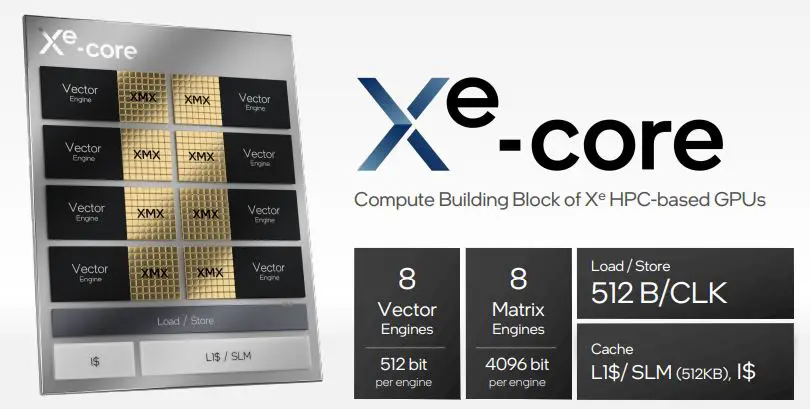
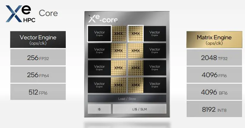
With regard to Xe-core, in Xe HPC we are dealing with a unit based on 8 Vector Engine and 8 Matrix Engine (XMX) supported by a load / store unit that can perform 512 bytes per clock fetching and large software configurable L1 cache. This unit is the basic building block of one slice, that is a unit formed by 16 Xe-cores, 8MB L1 cache and 16 ray tracing units, providing a single “hardware context” which allows multiple applications to run smoothly in parallel, enabling more effective use of the GPU in the cloud.
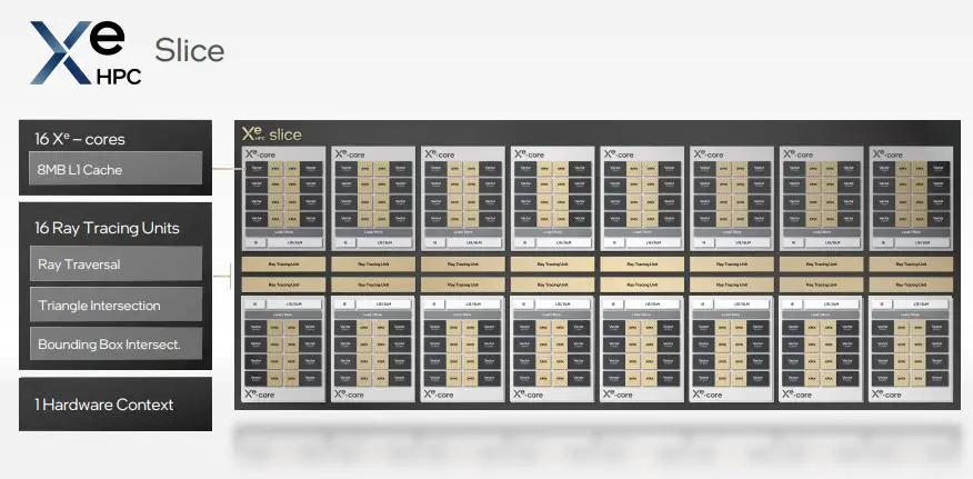
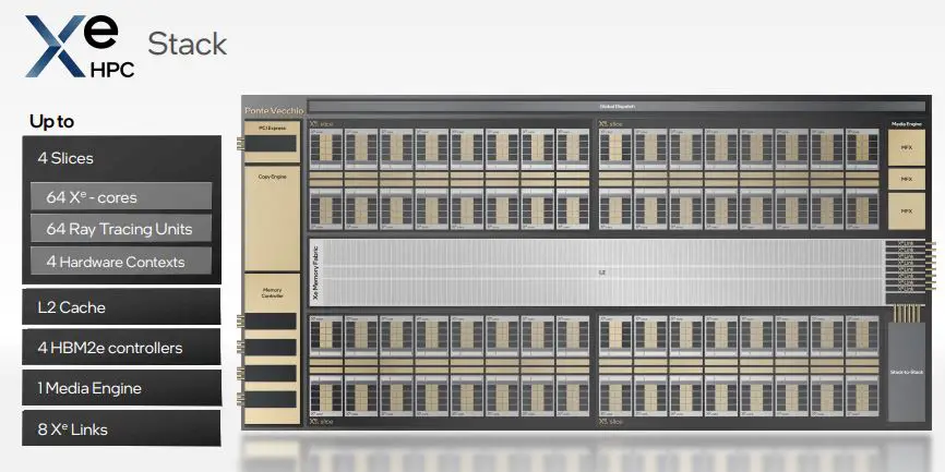
Going up to a higher level we come to stack, that matters 4 Slices for a total of 64 Xe-cores, 64 ray tracing units and 4 hardware context. A huge L2 cache, 4 HBM2e controllers, a media engine and 8 Xe Links complete the whole.
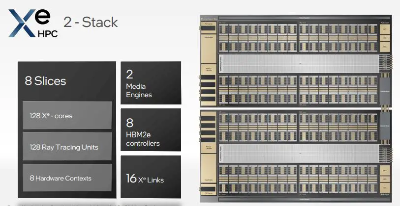
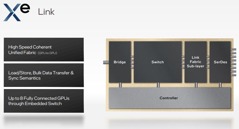
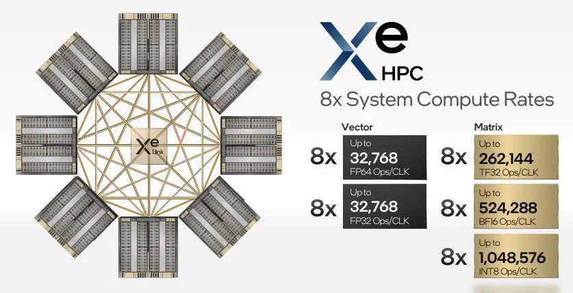
The architecture is though scalable, then Intel can create multi-stack design leveraging its EMIB packaging technology. Consequently, with 2 stacks Intel offers 128 Xe-cores, 128 ray tracing units, 8 hardware contexts, 2 media engines, 8 HBM2e controllers and 16 Xe Links, all while ensuring memory consistency between the stacks. Car Link is the link that allows one high-speed “GPU to GPU” communication and of connect up to 8 GPUs in one node without having to resort to external components.
And this is where we arrive at Ponte Vecchio, the concrete implementation of what Intel has conceived. Masooma Bhaiwala, chief engineer of Ponte Vecchio, said the “chip” is undoubtedly the most complex he has ever made in his career. “I don’t even know if we can call it a chip, it’s a collection of chips we call Tile, which work together through a high-bandwidth interconnect as a monolithic solution.” Ponte Vecchio is a product that has requested Intel of work from scratch on all aspects, from design to verification.
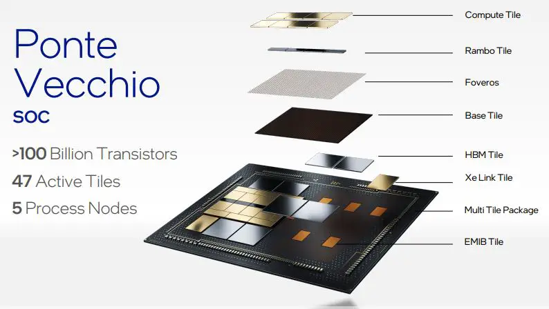
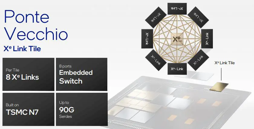
With over 100 billion transistors, 47 active tiles and the use of 5 different manufacturing processes, Ponte Vecchio is made up of Compute Tile, Rambo Tile, Foveros, Base Tile, HBM Tile, Xe Link Tile, Multi Tile Package ed EMIB Tile.
“Ponte Vecchio is composed of several complex elements that manifest themselves in tiles, which are then assembled through an EMIB tile that allows a low-power, high-speed connection between the tiles. These are assembled in the Foveros package that creates the 3D silicon stacking. active for power and interconnect density. A high-speed MDFI interconnect allows you to scale up from one to two stacks, “explained Bhaiwala.
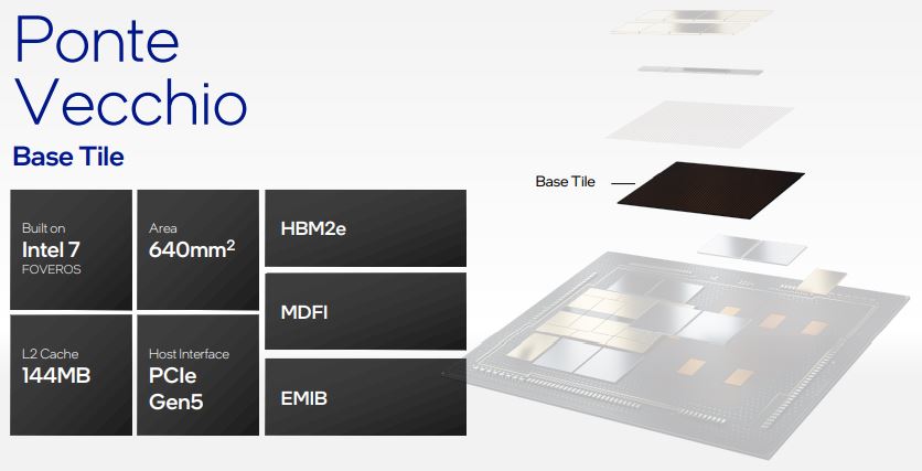
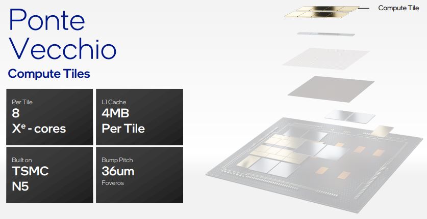
The Compute Tile It consists of 8 Xe-cores, has 4 MB of L1 cache and is produced by TSMC with N5 technology. There Base Tileinstead, it is made with Intel 7 process, occupies an area of 640 mm2, offers 144 MB of L2 cache and features a PCI Express 5.0 interface. Finally, Intel indicated that the Xe Link Tile is made by TSMC with N7 process.
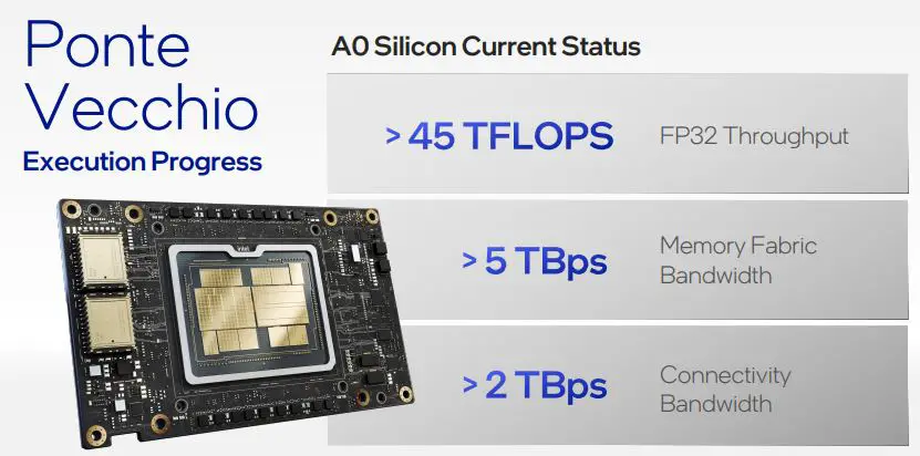
Intel’s first Ponte Vecchio chip built and tested has proven to deliver industry-leading performance, setting records in both inference and throughput on a commonly used AI benchmark. The performance of Intel’s A0 chip provides a throughput greater than 45 TFLOPS FP32, a memory fabric bandwidth of more than 5 TBps and a bandwidth for connectivity greater than 2 TBps.
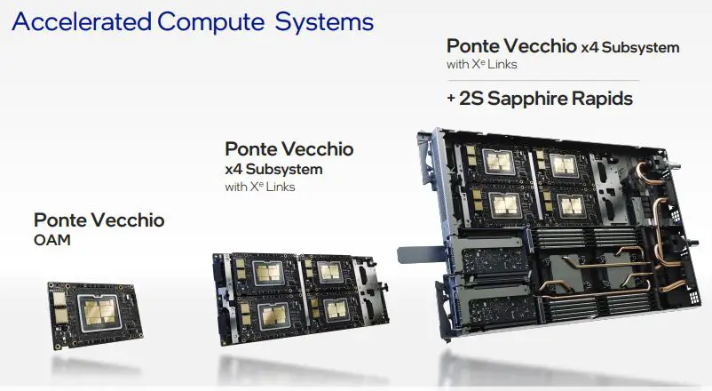
Ponte Vecchio is in production with the first samples, which are subjected to the validation phase, and the limited sampling phase for customers has started. It will be presented in 2022 for the HPC and AI markets where Intel is already preparing the ecosystem with oneAPI, a unified, cross-architecture and cross-vendor software stack, open and standards-based to enable single programming capable of running on multiple compute architectures.
Related posts:
 7-nanometer Nvidia GPU, TSMC will handle most of the production
  ASRock X299, a new BIOS allows you to install 2 TB of memory
  MSI Prestige X570 Creation Review: Test | Specs | Hashrate
  Radeon RX 5500 XT, PCI Express 3.0 castrates performance?
  An overclocker ran 1TB of RAM on an X299 motherboard limited to 256GB
  Best Review 2021: MSI MPG X570 Gaming Edge WiFi Under $250 ($200)