After several years of intensifying competition with Samsung, TSMC succeeded in being the first to introduce a 7-nanometer technology, something that has yielded results as most major players have flocked to the company at the expense of Samsung. One of these is AMD, which is investing heavily in 7 nanometers (7nm) exclusively at TSMC.
The industry magazine Digitimes reports that order intake for TSMC’s latest manufacturing technology has risen sharply. One of the reasons attributed is that more and more smart phones are being released with circuits produced at 7 nanometers. Specifically, there are two players mentioned – Hisilicon (Huawei) and AMD.
AMD currently has a product on the market that is manufactured on the technology and it is the graphics circuit Vega 20, which since the autumn of 2018 has been used in the Radeon Instinct MI50 and MI60. At the beginning of the year, AMD also launched the graphics circuit in Radeon VII, which is a gaming-oriented graphics card in the performance class for consumers.
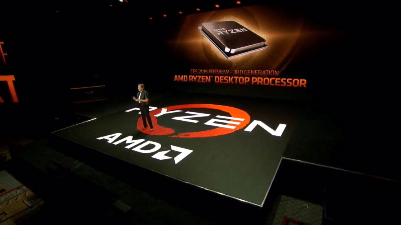
The fact that AMD is now really stepping up production at TSMC indicates that they are getting ready to launch the next generation of products. The process from a silicon wafer to finished circuits takes three months, which is in line with the company’s expectation to launch new processors in the Ryzen 3000 series with the Zen 2 architecture during the summer months.
In addition to a new generation of processors, AMD will use TSMC’s technology for the Navi graphics architecture. However, this is expected to be launched later in the year and in addition to new Radeon graphics cards, most point to Navi also laying the foundation for the next generation of game consoles from both Microsoft and Sony.
In parallel with increased order intake for current 7-nanometer technology, TSMC has recently started volume production of the refined variant 7nm +. This uses Extreme Ultraviolet Lithography (EUV), which cuts down on the number of steps in production and at the same time gives a higher proportion of working circuits (eng. Yield).
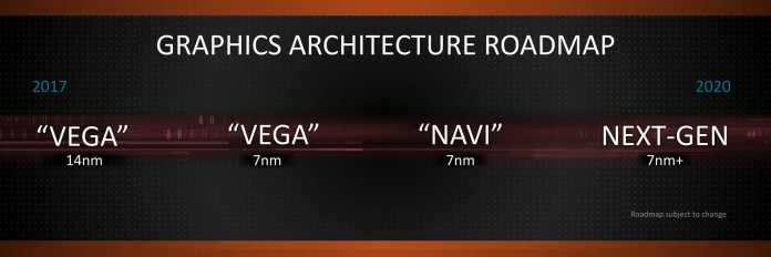
AMD will also use 7nm + for its next generation of products in 2020. According to TSMC, 7nm + will deliver 10 percent better energy efficiency to 17 percent higher transistor density, but in terms of potential clock frequency, the difference should be negligible compared to today’s 7nm. AMD also claims that Zen 3 at 7nm + will mainly be more energy efficient compared to Zen 2.
Read more about AMD’s upcoming products:
Related posts:
 Review & Test: Video card Gigabyte GeForce RTX 3060 Ti Gaming OC Pro
  AMD Radeon RX 5600 XT VS GTX 1660 Ti and RTX 2060: Review| Set-up| Hashrate
  Review of the KFA2 GeForce RTX 3060 Ti Core video card
  GIGABYTE GeForce RTX 3090 Gaming OC video card: Review| Specs | Set-up|
  INNO3D GeForce RTX 3090 iCHILL X4 video card review: Test | Config | Hashrate
  ROG Strix GeForce RTX 3070 OC Review: Test | Specs | Hashrate