AMD’s patent application for better GPU chiplet utilization
: Test |CUP | Specs |Config
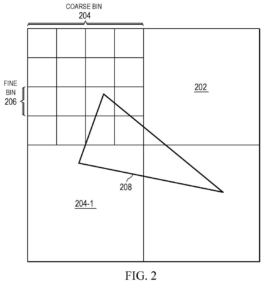
AMD has published a patent application for splitting the rendering load across multiple GPU chiplets, which provides some interesting insights. In order to optimize the utilization of the shaders in games, a game scene is divided into individual blocks and distributed to the chiplets. Two-level binning is used for this.
A whole wave of new patent applications
With a veritable spate of published patent applications over the past week, AMD has potentially revealed a lot of new insights into upcoming technologies in GPUs and CPUs. On June 30 alone, 54 patent applications were published. It remains to be seen which patents will ultimately be approved and which will actually be found in products. Regardless of this, the applications provide interesting insights into the technological approaches pursued by AMD.
Of particular interest is patent application US20220207827 for two-stage binning of image data in order to be able to better distribute the rendering loads of a GPU to several chiplets. AMD had already submitted the application at the end of December 2021.
The classic sharing of the load on shaders
Traditionally, the rasterization of image data on a GPU works relatively simply: Each shader unit (ALU) of the GPU can take on the same task, namely assigning a color to individual pixels. For this, the texture polygon located at the location of the corresponding pixel in the game scene is mapped onto the pixel. Since the calculation task is always the same in principle and only differs due to different textures at different points in the scene, the working method is called “single instruction – multiple data” (SIMD).
In modern games, this calculation step called “shading” is no longer the only task of a GPU. Instead, a lot of post-processing effects are now added as standard after the actual shading, which add, for example, environmental occlusion, anti-aliasing and shadows. Ray tracing, on the other hand, does not take place after shading, but parallel to it, and represents a completely different method of calculation. There is more about this in the report How GPU rays are accelerated.
In games on GPUs, this computing load scales up to several thousand computing units in an exemplary manner – unlike CPUs, where programs have to be written specially for more cores. This is made possible by the scheduler, which divides the work within the graphics card into smaller tasks that are processed by the compute units (CU). This division is called binning. To do this, the image to be rendered is divided into individual blocks with a certain number of pixels, each block is calculated by a sub-unit of the GPU and then synchronized and assembled. Pixels to be calculated are added to a block until the sub-unit of the graphics card is fully utilized. In this process, the computing power of the shaders, the memory bandwidth and the cache sizes are taken into account.
New challenges in multi-chiplet GPUs
As AMD points out in the patent text, the division and subsequent joining requires a very good data connection between the individual elements of a GPU. This is a hurdle for the chiplet strategy, since data links outside of a die are slower and have higher latencies.
While the transition to chiplets was relatively easy with CPUs, because a CPU task that has been divided up over several cores also works well on chiplets, this is not the case with GPUs. This means that a GPU’s scheduler today is where CPU software was before the introduction of the first dual-core CPUs. A fixed separation into several chiplets was previously not possible in a sensible way.
AMD’s approach: two-level binning
AMD aims to solve this problem by modifying the rasterization pipeline to split tasks across multiple GPU chiplets. For this purpose, the binning is expanded and improved. AMD speaks of “two-level binning” or “hybrid binning”.
Instead of dividing a game scene directly into blocks pixel by pixel, the division is carried out in two stages. First the geometry is processed, which means that the 3D scene is converted into a two-dimensional image. This step, called vertex shading, is usually done entirely before rasterization begins. In the case of GPU chiplets, the vertex shading is only minimally prepared on the first GPU chiplet and then the game scene is roughly binned. This creates coarse blocks (coarse bins), which are each processed by a GPU chiplet. Within these rough blocks, the vertex shading is completed, allowing traditional tasks such as rasterization and post-processing to take place.
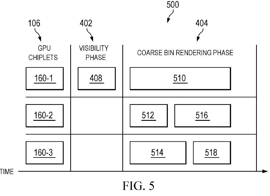
The chiplet that takes over the division is always the same and is called the “primary chiplet”. It is directly connected to the rest of the PC, primarily the CPU. The other chiplets take a back seat and only complete tasks when assigned to them. To do this, they work asynchronously and can continue to work even when the “Primary Chiplet” is busy analyzing the scene for the next frame (“Visibility Phase”). In general, it seems to be an enormous challenge to maximize the utilization of the processing units. While the “primary chiplet” is busy with the coarse binning of the game scene, the other units “wait” for data. If a chiplet finishes its block earlier than the rest, it waits again. That would be inefficient.
In order to optimize the utilization of the chiplets, AMD also provides a dynamic division in the patent in addition to a static division of the work (chiplet 1 always works on block 1, chiplet 2 on block 2, etc.). The workload of each block is estimated at the beginning in order to then distribute the blocks in such a way that all chiplets are completed at the same time. The two principles are illustrated in the figures contained in the patent “Fig. 4″ and “Fig. 5”.
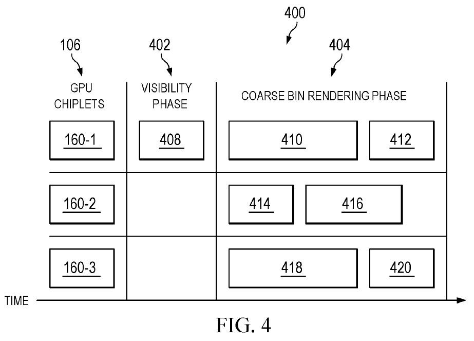
Static division of labor on GPU chiplets. Due to the different complexity of the tasks (410-420), the chiplets are completed at different times. (Image: AMD)
Bild 1 von 2
AMD’s approach also takes into account “simple” computing loads, where, for example, old games demand so little of the GPU that it would be uneconomical to split them up over several chiplets. Then the rasterization is completely taken over and processed by the first chiplet. There is no overhead and the remaining chiplets can be sent to an energy-saving state.
With its patent, AMD also protects a driver solution by describing a process via a “non-transitory computer readable medium”. The driver should provide instructions that enable the distribution of work to the GPU chiplets as described.
When will Radeon come with GPU chiplets?
There is currently no clarity as to when the approach described by AMD for optimized utilization of the shaders on multi-chiplet GPUs in games will become relevant in practice. AMD has meanwhile confirmed that RDNA 3 will be based on a chiplet approach as the basis of Radeon RX 7000 at the end of the year, but not that there will be several GPU chiplets. Recently it was said that although several memory controllers with Infinity Cache chiplets would be used, only one GPU chiplet would be used. Whether or not these rumors are true remains to be seen.
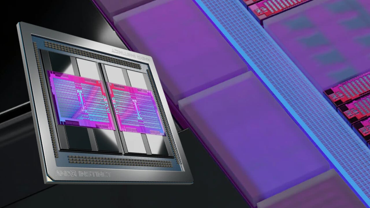
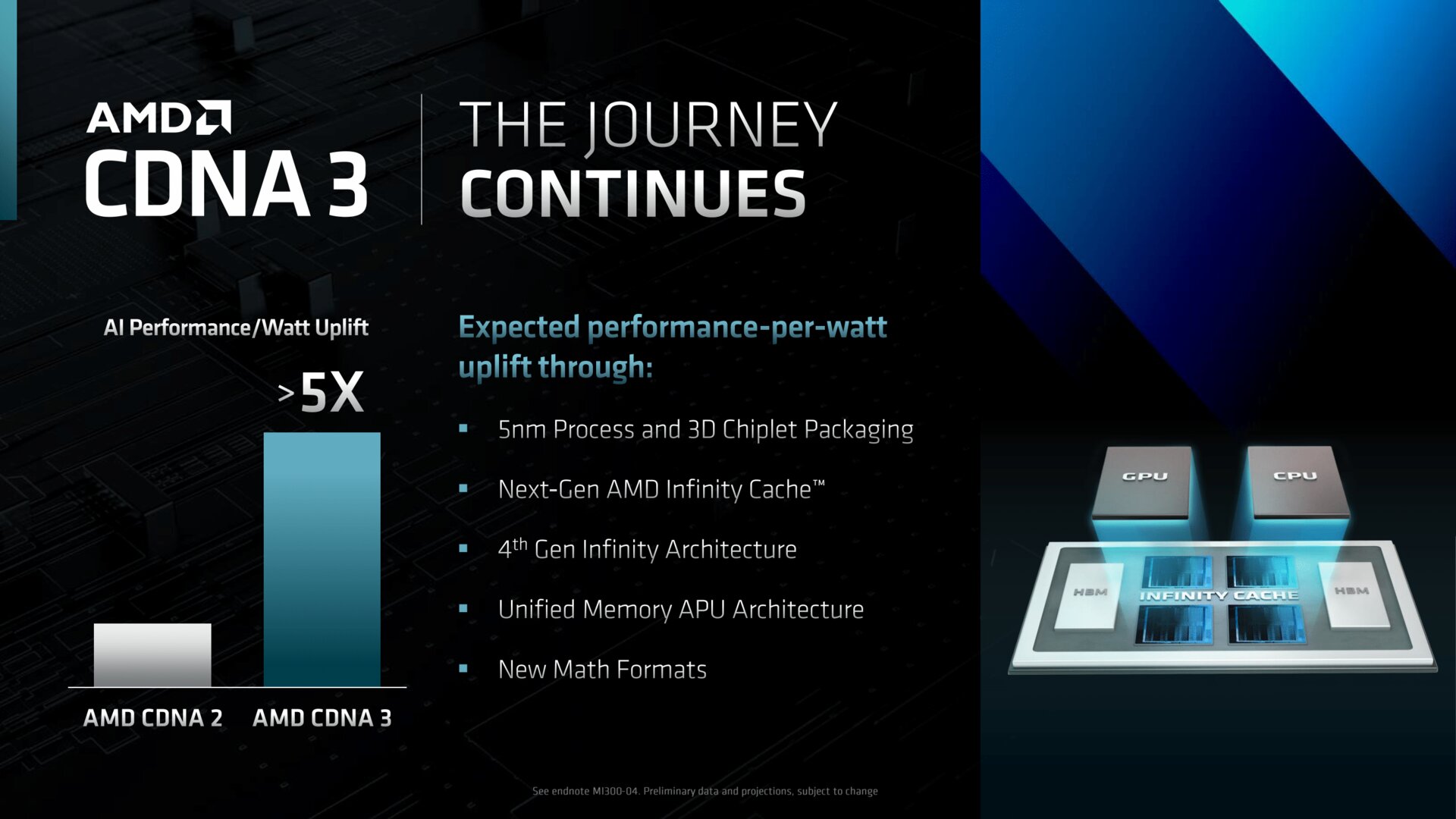
CDNA 2 already relies on two GCDs (Graphics Compute Dies) for the HPC graphics cards of the Instinct MI200 series, and CDNA 3 will build on them. The chiplets are connected via the “AMD Infinity Interconnect”.
- Radeon RX 7000 & MI300: RDNA 3 comes with chiplets, but only CDNA 3 stacks them
- AMD Radeon RX 7000: Navi 3X and RDNA 3 are planned as a hybrid in 5 and 6 nm
The editors would like to thank community member @ETI1120 for pointing this article out.
Was this article interesting, helpful or both? The editors are happy about any support from ComputerBase Pro and disabled ad blockers. More about ads on ComputerBase.
Related posts:
 7-nanometer Nvidia GPU, TSMC will handle most of the production
  ASRock X299, a new BIOS allows you to install 2 TB of memory
  MSI Prestige X570 Creation Review: Test | Specs | Hashrate
  Radeon RX 5500 XT, PCI Express 3.0 castrates performance?
  An overclocker ran 1TB of RAM on an X299 motherboard limited to 256GB
  Best Review 2021: MSI MPG X570 Gaming Edge WiFi Under $250 ($200)