A few days after its presentation at the International Conference on Solid State Circuits, Intel revealed all the details of its first Bitcoin mining ASIC based on its Bonanza Mine chips, capable of reaching an incredible 40TH/s with a consumption of 3600W,

To make these ASICs, the blue company uses 3 “hash boards” with 25 chips each, plus its regulation circuit and its digital control. In total there are 75 of these chips, which add up to a total of 40TH/s. In addition, there is an additional control board where there is an ARM chip where the mining program runs, and several FPGAs configured to communicate with the “hash boards”, sending information about what to process, and also controlling its temperature, voltage, and others. to see that everything is in order.
Compared to the competition, the power efficiency of these early Bonanza Mine chips leaves a lot to be desired. Bitmain’s Antminer S19j Pro 104T reaches 104TH/s with 3068W, while its successor the S19j XP reaches 140TH/s with 3010W. Intel revealed that it is aware of this, and that later this year it will release Bonanza Mine 2, with much more competitive energy efficiency. These BM2 chips are already reserved by companies like ARGO Blockchain, GRIID Infrastructure, and BLOCK, backed by Twitter CEO Jack Dorsey, so it looks like they will be competitive if they already have reserves from these big mining companies.
Intel will provide more details on Bonanza Mine this coming Wednesday at the International Solid State Circuits Conference, so keep an eye out for new information.
What do you think about this new Intel ASIC based on its Bonanza Mine chips? Do you think that in the second generation they will be more competitive?
Source: Tom’s Hardware
Related posts:
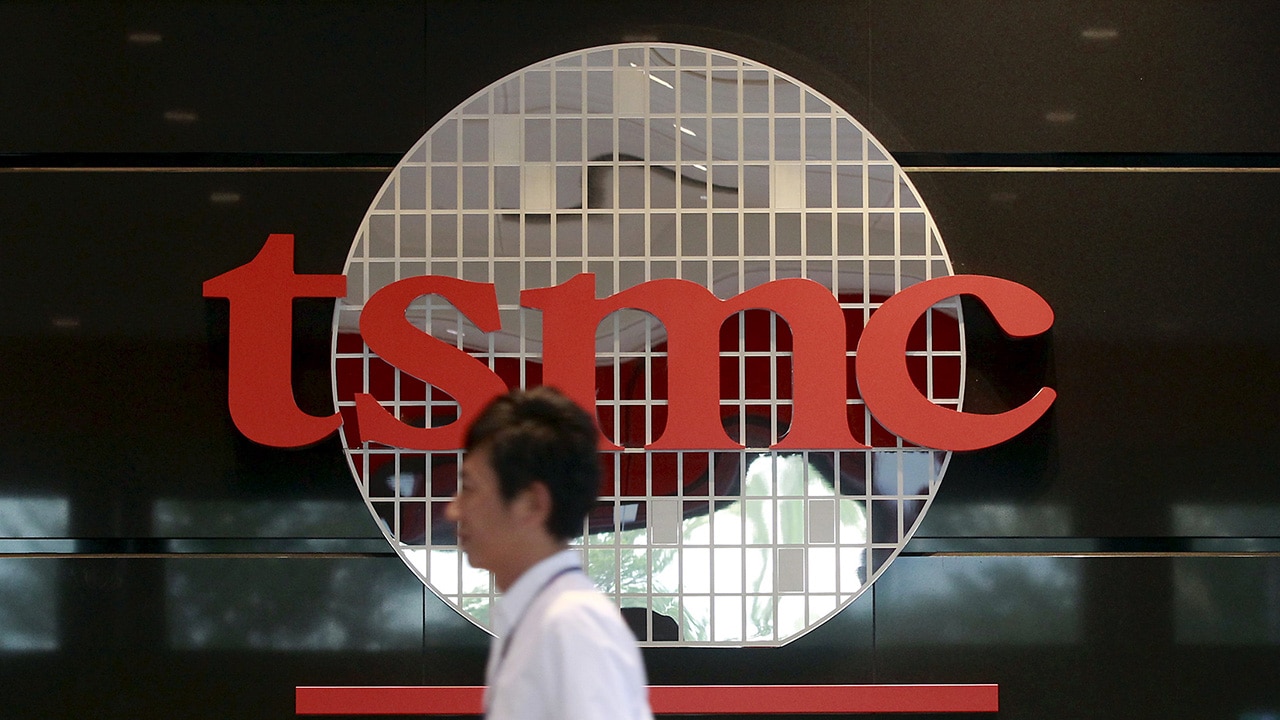
 7-nanometer Nvidia GPU, TSMC will handle most of the production
  ASRock X299, a new BIOS allows you to install 2 TB of memory
  MSI Prestige X570 Creation Review: Test | Specs | Hashrate
 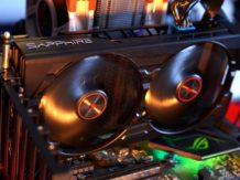 Radeon RX 5500 XT, PCI Express 3.0 castrates performance?
 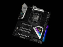 An overclocker ran 1TB of RAM on an X299 motherboard limited to 256GB
 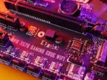 Best Review 2021: MSI MPG X570 Gaming Edge WiFi Under $250 ($200)