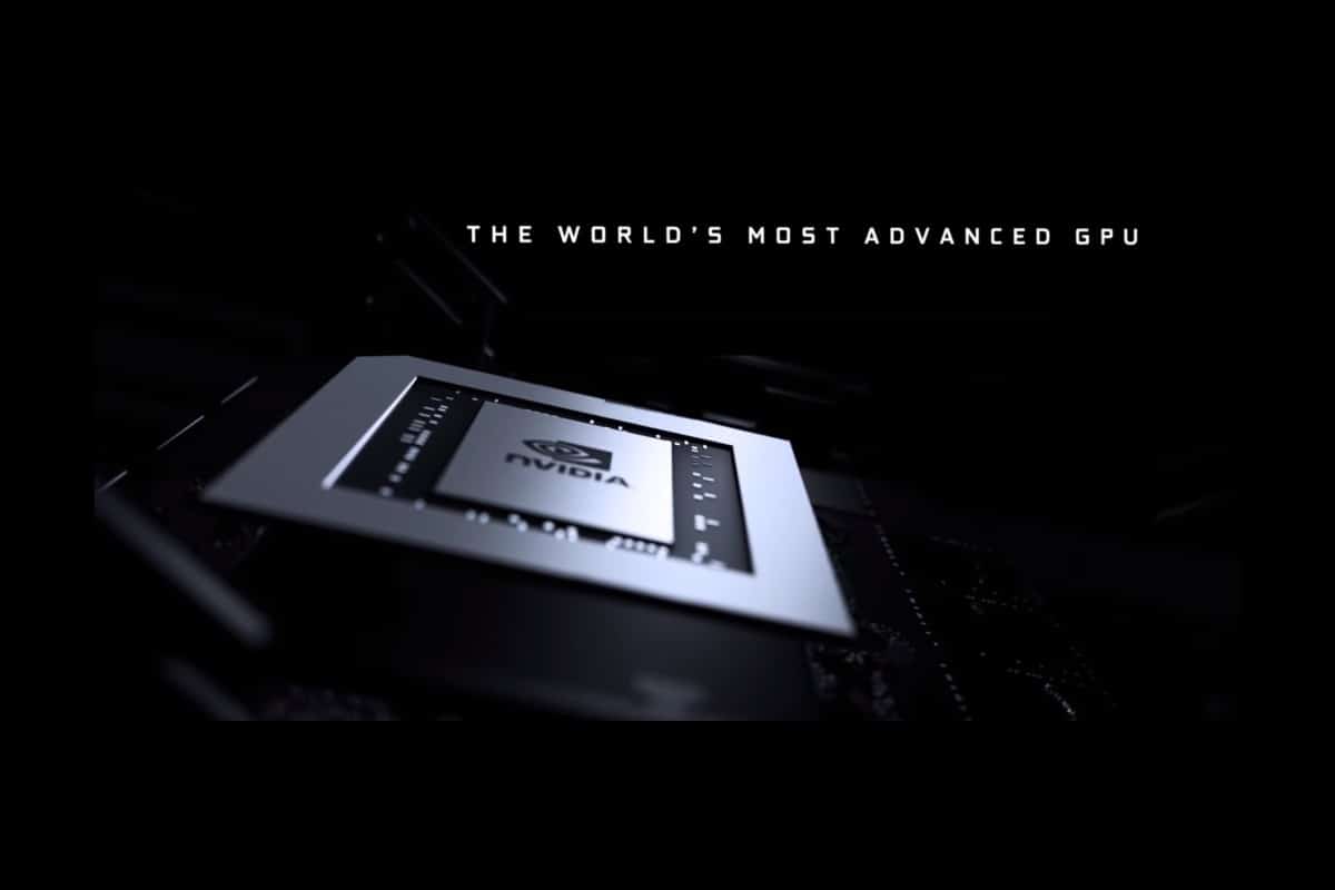
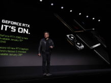
NVIDIA has finally removed the veils on architecture GPU Ampere at 7nm, eagerly awaited by professionals and certainly a new reference point for professional graphics, without forgetting the consumer graphics cards for gaming that will come later (see the much talked about GeForce RTX 3000 series).
As often happens in these cases, the Ampere architecture debuts first on the professional segment, in this case we talk about the GPU Ampere A100 that will equip the professional card (or rather HPC) Tesla A100. Ampere A100 is the most impressive GPU ever designed, not only for size but especially for the performance which, according to NVIDIA, in AI they are 20 times higher than the previous generation (based on the scenario).
But let's get to the numbers of this new GPU which, thanks to the renewed 7-nanometer production process, has made it possible to integrate 54 billion transistors is 6912 Cuda Core in a single chip (108 SM – Streaming Multiprocessor) with an area of 826 mm². The latest generation of HBM memory is used (HBM2E to be precise, announced in February), with the possibility of using 40GB of VRAM.
Memory interfaces with the GPU with a 5120 bit bus, while the NVLink third generation support which allows a GPU / GPU interconnection speed of 600 GB / s. Going back to the new Tesla A100, let's talk about a card that arrives in SMX3 format with a 400W TDP, a sign that this type of solution is very demanding in terms of energy despite the GPU being built at 7nm. These at the moment the first details, we await further updates, especially to know the plans of NVIDIA regarding consumer proposals.
TECHNICAL CHARACTERISTICS NVIDIA TESLA A100
- NVIDIA Ampere GA100 GPU
- Dimensions of 826 mm²
- Transistor 54 billion
- Multi-Processor Streaming (SM) 108
- Cuda Core 6912
- 432 Third Generation Tensor Core with TF32
- GPU boost frequency 1410 MHz
- 40GB HBM2E memory
- 1250 MHz memory data-rate
- 5120 bit memory bus
- Memory bandwidth 1.6 TB / s
- PCI-E gen 4.0 interface
- TDP 400W
- Performance 19.5 TFLOPS (FP32)
Related posts:
 7-nanometer Nvidia GPU, TSMC will handle most of the production
  ASRock X299, a new BIOS allows you to install 2 TB of memory
  MSI Prestige X570 Creation Review: Test | Specs | Hashrate
  Radeon RX 5500 XT, PCI Express 3.0 castrates performance?
  An overclocker ran 1TB of RAM on an X299 motherboard limited to 256GB
 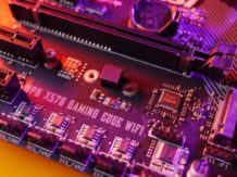 Best Review 2021: MSI MPG X570 Gaming Edge WiFi Under $250 ($200)