
Recently during the GTC conference, the scientific Nvidia boss Bill Dally discussed how his R&D (Research and Development) teams are using AI to speed up and improve the design of new GPUs. Four complex and traditionally slow processes have already been realized by leveraging machine learning (ML) and artificial intelligence techniques (IA). In one example, using accelerated AI/ML can speed up a GPU layout task from three hours to three seconds.
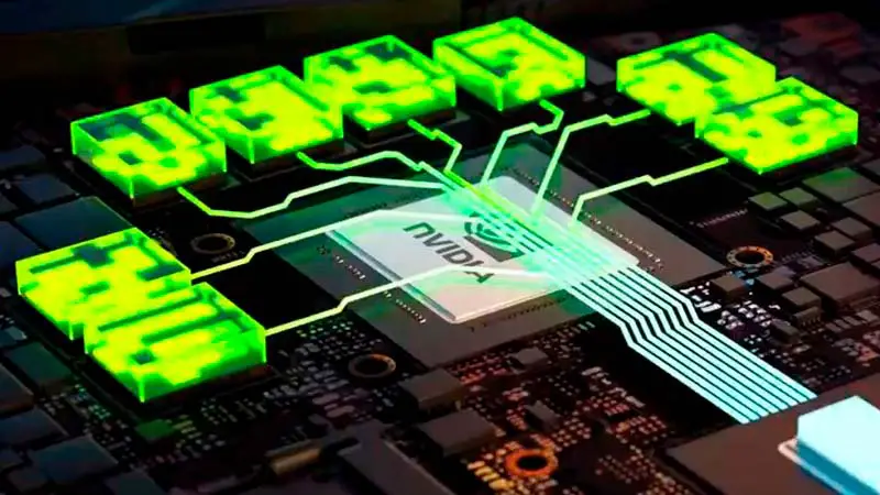
Dally supervises about 300 people, and these people usually work in research groups as shown in the image below:
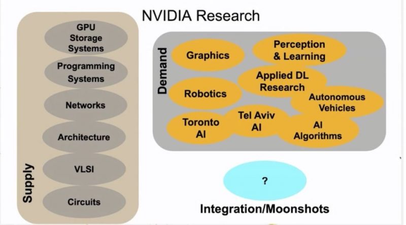
In his talk, Dally outlined four important areas of GPU design where AI/ML can be leveraged to great effect: voltage drop mapping, stray emission prediction, location and routing challenges, and automation of data migration. standard cells. Let’s take a look at each process and how AI tools are helping Nvidia R&D run more efficiently.
What is R&D? It is research and development, it is the research process in scientific and technical knowledge, with the aim of developing technologies to obtain new products, materials or processes.
The benefits of using AI (Artificial Intelligence)
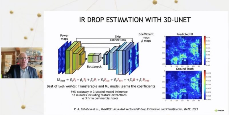
Voltage Drop Mapping
Voltage drop mapping helps designers see where power flow travels in next-generation GPU designs. Using a conventional CAD tool will help them calculate these numbers in about three hours, says Dally. However, once trained, NVIDIA’s AI tool can reduce this process to three seconds. The process, in its current state, offers an accuracy of 94%.
parasitic prediction
Predicting parasites using AI is particularly enjoyable for Dally. As a circuit designer, he spent long periods with his colleagues anticipating parasites in the development process, and this new AI model reduces a time-consuming, multi-person, multi-skill process. Again, the simulation error is reasonably low, less than 10% in this case. Reducing these traditionally lengthy iterative processes can free up a circuit designer to be more creative in other activities.
Parasitic prediction studies the electrical capacity caused by unwanted phenomena in a circuit or system.

Location and routing challenges
Location and routing challenges are important to chip design, as they are like planning roads in a busy city. Getting this wrong will pay off poorly as poor data flow can reduce efficiency exponentially, requiring rerouting or replanning designs for higher efficiency. Using Graph Neural Networks (GNN) to analyze this problem in the chip design helps highlight potential problem areas and act on them intelligently.
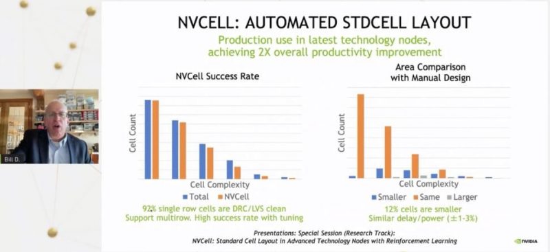
Automation of standard cell migration
Finally, automating standard cell migration using AI is another very useful tool in Nvidia’s chip design toolbox. Dally talks about the enormous effort previously required to migrate a chip design from seven to five nanometers, for example. Using AI, Dally claims that “92% of the cell library could be done with this tool with no design rules or electrical rule errors” and that “in many cases, they ended up with a better design”
Last year at GTC, Dally’s talk emphasized how NVIDIA planned to prioritize AI and talked about Nvidia’s five separate labs that are dedicated to AI research projects.
Dally says that all this should already be polished to develop the new 7nm and 5nm graphics cards, in addition NVIDIA will include the Ada Lovelace line in these new projects.
Related posts:
 7-nanometer Nvidia GPU, TSMC will handle most of the production
  ASRock X299, a new BIOS allows you to install 2 TB of memory
  MSI Prestige X570 Creation Review: Test | Specs | Hashrate
  Radeon RX 5500 XT, PCI Express 3.0 castrates performance?
  An overclocker ran 1TB of RAM on an X299 motherboard limited to 256GB
  Best Review 2021: MSI MPG X570 Gaming Edge WiFi Under $250 ($200)