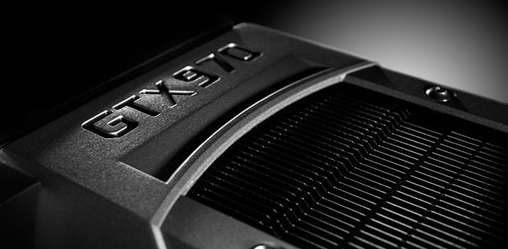
Anyone who surfed SweClockers this weekend has probably not missed all the inflamed discussions about the Geforce GTX 970. The popular graphics card contains a scaled-down variant of the GM204 circuit, which for a hitherto unclear reason divides the 4 GB large video memory into two segments of 3.5 and 0.5 GB. What the controversy is about is that the smaller piece is pulled with significantly lower bandwidth than normal.
Nvidia corrects * specifications * for Geforce GTX 970
GTX 980 | GTX 970 (older) | GTX 970 (new) | |
|---|---|---|---|
Technical | 28 nm | 28 nm | 28 nm |
GPU | GM204 | GM204 | GM204 |
Transistors | 5,2 md | 5,2 md | 5,2 md |
Circuit area 398 mm2 | 398 mm2 | 398 mm2 | 398 mm2 |
Architecture | Maxwell | Maxwell | Maxwell |
CUDA cores | 2 048 st. | 1 664 st. | 1 664 st. |
Texture units | 128 st. | 128 st. | 128 st. |
Raster units | 64 st. | 64 st. | 56 st. |
Bass frequency | 1 126 MHz | 1 050 MHz | 1 050 MHz |
Turbo frequency | 1 216 MHz | 1 178 MHz | 1 178 MHz |
L2 cache memory | 2 MB | 2 MB | 1,75 MB |
Memory bus | 256-bit | 256-bit | 256-bit |
Memory amount | 4 GB GDDR5 | 4 GB GDDR5 | 4 GB GDDR5 |
Memory frequency | 7 000 MHz | 7 000 MHz | 7 000 MHz |
Memory bandwidth | 224 GB/s | 224 GB/s | 224 GB/s (?) |
Power supply | 6+6-pin | 6+6-pin | 6+6-pin |
TDP | 165 W | 148 W | 148 W |
Following the first official statement, Nvidia provides a more in-depth explanation of the phenomenon. Contrary to many theories, the behavior is not directly related to the fact that the Geforce GTX 970 lacks three so-called SMM cluster compared to big brother GTX 980. The graphics circuit is divided into two sections, where the communication is handled by what Nvidia calls a crossbar or crossbeam.
In the upper part of the diagram, CUDA cores are visible in SMM clusters, at the same time as video memory management and L2 cache memory are housed on the other side of the crossbar. According to Nvidia, it provides, among other things, flexibility for handling partially defective circuits, where different parts can be deactivated independently of each other without affecting communication.
Slimming down GM204 affects memory bandwidth
New for the Maxwell generation is that not only computational clusters can be disabled if needed but also parts of the logic for memory management, something that for Kepler required that the entire section be scrapped. In practice, this means that the Geforce GTX 970 lacks a set of L2 caches and the associated connection to the crossbar compared to the big brother GTX 980.
two different sections of memory
In short, the result is that a single port with associated logic becomes responsible for handling two memory channels, something that can in principle halve the performance. Nvidia’s solution to the problem is to segment the video memory into two sections, where 3.5 GB is always available while the remaining 0.5 GB is only used when needed.
The 3.5 GB section of video memory has access to 7 memory channels, which broadly provides 7 / 8ths of the bandwidth compared to the Geforce GTX 980. However, the last segment only gets access to 1 / 8th of the maximum bandwidth.
The handling of the segments, or rather the optimization, is handled in Nvidia’s driver and in the operating system. The software actively tries and as far as possible to use the faster 3.5 GB section. When more space is needed for a single operation, the last 0.5 GB is used, which is still faster than, for example, working towards the primary memory.
Nvidia claims that the effect of it all in most cases is a minimal loss of performance compared to if all the video memory always worked at full speed. However, the graphics card maker promises to investigate any issues reported by concerned users and possibly make further optimizations of the memory management in the drivers.
* To reflect the memory management in the Geforce GTX 970, Nvidia also updates the graphics card’s specifications, where the number of raster units now amounts to 56, while the L2 cache is reduced to 1.75 MB.
Related posts:
 Review & Test: Video card Gigabyte GeForce RTX 3060 Ti Gaming OC Pro
  AMD Radeon RX 5600 XT VS GTX 1660 Ti and RTX 2060: Review| Set-up| Hashrate
  Review of the KFA2 GeForce RTX 3060 Ti Core video card
 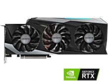 GIGABYTE GeForce RTX 3090 Gaming OC video card: Review| Specs | Set-up|
  INNO3D GeForce RTX 3090 iCHILL X4 video card review: Test | Config | Hashrate
 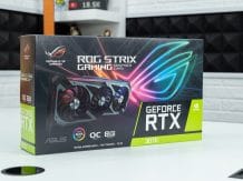 ROG Strix GeForce RTX 3070 OC Review: Test | Specs | Hashrate