Nvidia GA100 (Ampere) im Detail
: Test |CUP | Specs |Config
tl;dr: Nvidia’s A100, the first product with Ampere architecture, is intended for AI calculations in the data center. The basis is the gigantic GA100-GPU with 826 mm². The article clarifies what its full expansion has to offer, how it compares to Volta and what can be derived from amps for GeForce – as far as possible.
GA100: The surprise behind A100
Actually everything was clear: On Thursday afternoon, the presentation of Nvidias for the data center and the A100 accelerator specially designed for AI training and inferencing should take place. ComputerBase had received information from Nvidia under NDA in advance in order to prepare an article. It was astonishing that there were only relatively few details about its technology. But it seemed clear: only A100 in various versions will be the topic in the recorded keynote. But it turned out differently.
At the same time as the presentation of the A100, Nvidia put a comprehensive article on the A100 online, which revealed a lot more about the new Ampere architecture, and it turned out that the GPU of the A100 is not called A100 at all, but that the manufacturer follows the old scheme and it GA100 has baptized. And then there were detailed technical details about exactly this GPU.
It was no surprise that the A100 does not use the full configuration of the GA100 GPU. That was the case with the Tesla V100 and the GV100-GPU and is the rule in this segment: Especially with such huge GPUs, it can quickly happen that not all units function correctly, and execution units that are scheduled to be switched off can significantly reduce chip waste. What is unusual about the GA100, however, is that Nvidia has switched off 15 percent of all units – including an entire HBM2 stack, including memory chips and bandwidth. The cut is enormous and knowing it automatically makes the GA100 even more impressive than the A100 already was.
This is the fully activated GA100
The GA100 is a huge GPU: it occupies 826 mm², is manufactured using the N7 process at TSMC and comprises 54.2 billion transistors. An AMD Ryzen Threadripper 3990X with 64 cores distributed over 8 CPU dies and one I / O die “only” reaches 40 billion. Compared to Volta, the number has more than doubled. The question was therefore whether the numerous AI improvements in the A100 alone required so many transistors. Now that it is known what is really behind the GA100, the numbers suddenly make a lot more sense.
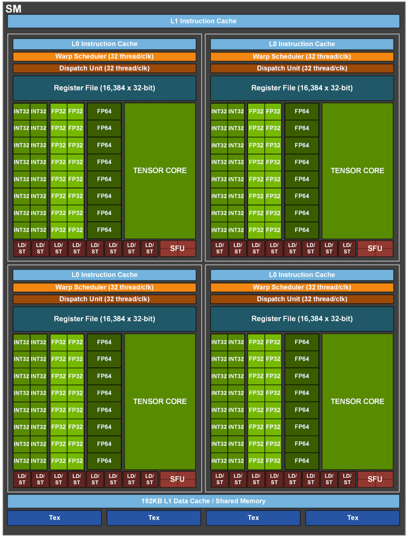
Because the GA100 has more than the 108 streaming multiprocessors and thus the 6,912 FP32-ALUs of the A100. There are even 128 SMs and thus 8,192 ALUs. This would enable an additional 18 percent of execution units to be activated, if intact and desired. The GA100 automatically not only has more FP32-ALUs, it also has many more units to scale. The seven graphics processing clusters (GPC, quasi an entire computing block consisting of ALUs, TMUs and much more) become 8, 3,456 FP64-ALUs become 4,096, 432 tensor cores become 512, 432 texture units become 512 and also the The entire geometry block including the caches connected to the SMs is correspondingly larger. And that’s not the end of the story, because the A100 is nowhere near going to full capacity when it comes to storage either.
Because while the A100 “only” offers 5 HBM2 stacks with 8 GB each and a memory interface totaling 5,120 bits (1,024 bits per stack), the GA100 can also handle 6 stacks, 48 GB and 6,144 bits. So there are even greater reserves in the memory than in the arithmetic units: 20 percent.
Why is so much disabled?
The question arises as to why Nvidia disabled so many units. That cannot be clarified at this point, there are no official statements. Two motivations are possible: On the one hand, Nvidia certainly does without with amps what the Californians have done with the last professional GPU generations: the full expansion in order to still be able to sell partially defective chips.
This is especially advisable with huge and complex chips like the GA100, because the same number of production defects per wafer affects a larger proportion of the GPUs on the wafer. However, it is unusual to turn off a fifth of the chip.
With the predecessor Volta, the GV100, 80 of 84 SMs were activated and thus only 5 percent of the units were switched off. Even if Nvidia needed a larger buffer due to the different production, the one from the GA100 seems too big. In addition, this would not explain why an HBM2 stack is also not occupied. Because that reduces the memory bandwidth, which is so important in the HPC segment, enormously.
Therefore, a second background seems quite realistic: The A100 will only be the beginning with GA100 and Nvidia is planning a faster version of the professional graphics card in the future. Quasi the super model for professionals. This is rather unusual in the segment, but at some point there is a beginning for everything. And it does not contradict the committee argument. Perhaps the production of the huge 7 nm GPU is still a bit problematic at the moment, but Nvidia is assuming that it will be much better in the future. Until then you could sell a lot of A100 and with a better yield you would later have the market for an “A200”.
Ampere vs. Volta from a bird’s eye view
Nvidia has not made any changes to the basic structure of Ampere compared to Turing – according to the current status. The division of the GPU into GPCs, TPCs and SMs has remained the same and this also applies to the units in these main categories. The block diagram is very similar to that of Turing.
Cache improvements
Nvidia has made some improvements to the cache on the GA100. The L1 cache and the shared memory per SM have grown from 128 to 192 KB compared to Volta, and the L1 cache alone in the GA100 has a total of almost 25 MB. The cache should also have become faster, but Nvidia does not provide any information.
The L2 cache makes a significantly larger jump. While it was 6 MB with the Volta, it is 40 MB with the GA100 – almost seven times as much. The L2 cache is divided into two different partitions, which improves bandwidth and access times. In addition, Nvidia has also modified the crossbar of the cache, which connects the fast cache with the SMs, so that the read rate of the cache should be 2.3 times as high as with Volta. In addition, it should now be easier for the programmer to determine which data should be in the cache and which should not.
The tensor cores are now 4 times as fast as with Volta
It sounds astonishing that the A100 with only 432 tensor cores should be able to calculate matrices significantly faster than the predecessor Tesla V100 with Volta with at least 640 tensor cores. The message is clear: The tensor cores are much faster.
Volta (and Turing) has 8 tensor cores per SM, each of which can perform 64 FP16 / FP32 Mixed-Precision Fused Multiply-Add (FMA). With amps there are only 4 tensor cores per SM, which can, however, carry out 256 FP16 / FP32 FMA operations per cycle. Despite only half as many tensor cores per SM, the die output at amperes has doubled compared to its predecessor. Since the GA100 also has more SMs, this results in the significantly increased AI performance.
For more details on Ampere’s AI capabilities, a look at the report on the A100 derivative is recommended.
Calculating graphics is possible, but not ray tracing
It currently seems certain that AMD’s new professional GPU Arcturus cannot calculate graphics and will concentrate purely on HPC tasks. This is not the case with Ampere, at least Nvidia also speaks of “graphics rendering” and “cloud gaming”. In addition, the block diagram shows the texture units necessary for playing. The geometry units and the ROPs, which are also required for the graphic calculation, are missing. However, Nvidia had already omitted their representation in the Volta block diagram. So they are presumably there, but they do not play a role in the application area of the A100.
What is also missing from the block diagram of the GA100 are the ray tracing units. Nvidia has meanwhile also confirmed that the GA100 does not have any ray tracing units. The same applies to the video unit NVENC. The reason given by Nvidia is that both are simply not needed when using HPC. The same applies to monitor connections.
What does the GA100 mean for gamers?
With its sheer size, mass of execution units and large caches, GA100 is undoubtedly exciting. But with the idea of Ampere, the question also arises, what can be derived from the professional GPU for the gaming graphics cards of the GeForce series with the “GeForce RTX 3080 Ti”, which is already used as the headline in many places? If you are honest the answer is: very little.
The new GeForce RTX graphics cards (and GTX?) Will also be based on amps, the basis between the GPUs for professionals and gamers is the same. It was the same with Volta and Turing. All amps improvements in areas relevant to gaming GPUs will also be received by gamers. These include, for example, improvements to the tensor cores (DLSS, denoising at RTX) and the cache. What is still completely unclear is to what extent the ALUs have become faster apart from the tensor cores and what about the speed and number of RT cores. It is also unclear whether something has been done with the front end, the geometry units, the TMUs or the ROPs. And whether TSMC’s 7-nm process is used, and if so, in what form, is still just a guess.
What is certain, however, is that “gaming amps” will have a completely different configuration than professional amps. So the gamer’s graphics card will definitely receive significantly fewer shader units and everything related to them. In contrast to this, the clock rate will definitely increase significantly and again be at least around 2.0 GHz instead of 1410 MHz on the A100. There will probably also be major cuts in the cache.
Virtually everything should change when it comes to storage. The player will hardly get HBM2, instead 18 Gbps (9,000 MHz) faster GDDR6 memory is used. This means that the memory bandwidth will be significantly lower, but it should be enough for games.
How ray tracing will change is still a mystery
While the GA100 completely dispenses with ray tracing units, the GeForce RTX 3000 offshoots will definitely upgrade significantly compared to Turing in this regard. It remains to be seen whether this simply means significantly more RT cores, significantly improved RT cores, both or possibly something like the tensor cores (fewer, but significantly better cores).
The date of publication is and remains just as unclear. At the moment everything still points to a market launch this year. However, no reliable information is available yet as to whether this will happen in the third or (more likely) in the fourth quarter. ComputerBase will pick up on well-founded rumors on this topic over the coming months, but will not chase every allegedly authentic leak on GeForce RTX 3000.
Was this article interesting, helpful, or both? The editors appreciate every support from ComputerBase Pro and deactivated ad blockers. More about advertisements on ComputerBase.
Related posts:
 7-nanometer Nvidia GPU, TSMC will handle most of the production
  ASRock X299, a new BIOS allows you to install 2 TB of memory
  MSI Prestige X570 Creation Review: Test | Specs | Hashrate
  Radeon RX 5500 XT, PCI Express 3.0 castrates performance?
  An overclocker ran 1TB of RAM on an X299 motherboard limited to 256GB
  Best Review 2021: MSI MPG X570 Gaming Edge WiFi Under $250 ($200)