Samsung Electronics has announced that it has developed the first technology to stack up to 12 DRAM memory chips. We are talking about a technology 3D-TSV (Through Silicon Via) 12-layer, with vertical interconnections that connect 12 DRAM chips together thanks to over 60,000 TSV holes with a width of one twentieth the thickness of a human hair.
The thickness of the package is 720 micrometers, the same as the current products with 8 layers of High Bandwidth Memory 2 (HBM2). In this way the next generation products will be able to offer more performance and memory capacity without changing your design.
The 3D packaging technology also features a better data transmission time between the chips compared to that guaranteed by the current “wire bonding” technology, thus ensuring lower consumption and higher speeds.

Thanks to the possibility of increasing the number of stacked layers from 8 to 12, Samsung will be soon able to produce HBM memory in volumes up to 24 GB. “A packaging technology that addresses all the complexities of high performance memory is becoming tremendously important, with the possibility of being used in new sectors such as artificial intelligence (AI) and high power computing (HPC)”, said Hong-Joo Baek, executive vice president of Samsung Electronics' TSP (Test & System Package) group.
“With the scaling of Moore's Law reaching its limits, the role of 3D-TSV technology is expected to become even more central. We want to be at the forefront of this state-of-the-art packaging technology. “
Related posts:
 7-nanometer Nvidia GPU, TSMC will handle most of the production
 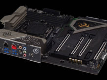 ASRock X299, a new BIOS allows you to install 2 TB of memory
 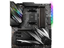 MSI Prestige X570 Creation Review: Test | Specs | Hashrate
  Radeon RX 5500 XT, PCI Express 3.0 castrates performance?
 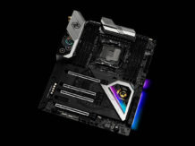 An overclocker ran 1TB of RAM on an X299 motherboard limited to 256GB
 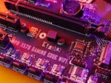 Best Review 2021: MSI MPG X570 Gaming Edge WiFi Under $250 ($200)