At GTC 2022, Nvidia revealed details of its Hopper architecture and Nvidia H100 GPU. The Hopper architecture and H100 GPU should not be confused with Ada Lovelace, the consumer-focused architecture that will power future GeForce cards.
The Hopper H100 will replace the Ampere A100, which replaced the Volta V100. This is data center hardware, and with fierce competition from manufacturers like AMD’s Instinct MI250/250X cards and the recently announced Instinct MI210, Nvidia is looking to retake the lead in high-performance computing.
Unsurprisingly, the H100 was designed for supercomputers with a focus on AI capabilities. It includes numerous updates to and from the current A100, all designed to reach new levels of performance and efficiency.
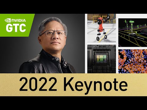
GTC 2022 Keynote with NVIDIA CEO Jensen Huang
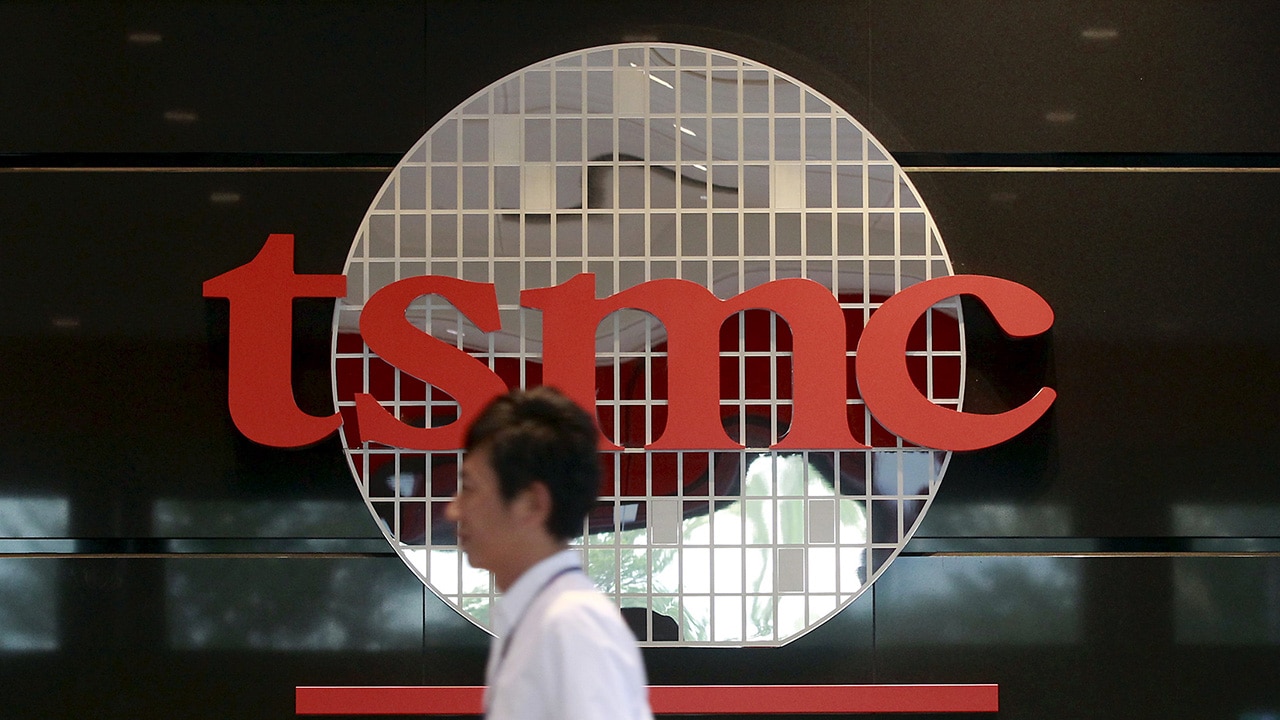
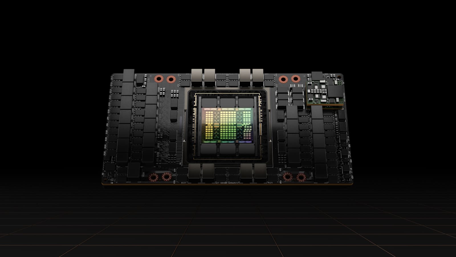
Hopper contains 80 billion transistors and is built using a process called TSMC’s custom 4nm N4 process, slightly different from the 4nm N4 process also offered by TSMC. For comparison, the A100 GPU had only 54 billion transistors.
Nvidia hasn’t revealed the GPU speed on the new card, but has given some other details. The H100 supports Nvidia’s fourth-generation NVLink interface, which can provide up to 128GB/s of bandwidth. It also supports PCIe 5.0 for systems not using NVLink, which also tops out at 128GB/s. The updated NVLink connection provides 1.5 times more bandwidth than the A100, while PCIe 5.0 offers twice the bandwidth of PCIe 4.0.
A huge leap in performance.
The H100 will also support 80GB of HBM memory, with 3TB/s of bandwidth, that’s 1.5 times faster than the A100’s HBM2E. While the A100 was available in 40GB and 80GB models, both the H100 and A100 still use up to six stacks of HBM modules. Overall, the H100 has 50% more memory and bandwidth compared to its predecessor.
That’s a nice improvement, but other aspects of the Hopper GPU mean even bigger improvements. The H100 can deliver up to 2,000 TFLOPS of FP16 compute and 1,000 TFLOPS of TF32 compute, as well as 60 TFLOPS of general-purpose FP64 compute, triple the performance of the A100 in all three cases.
The Hopper GPU also adds improved support for FP8 with up to 4000 TFLOPS of compute, six times faster than the A100 (which had to rely on FP16 as it didn’t have native FP8 support). To help optimize performance, Nvidia also has a new transformer engine that automatically switches between FP8 and FP16 formats based on workload.
Nvidia has also added new DPX instructions designed to speed up dynamic programming. This can help with a wide variety of algorithms, including path optimization and genomics, and Nvidia claims the performance of these algorithms is up to 7x faster on Hopper H100 than previous generation GPUs, and up to 40x faster than before. State-of-the-art GPU CPU-based algorithms. Hopper also includes changes to improve security, and in GPU virtualization systems it now allows seven secure instances to run on a single H100 GPU.
what about consumption
All of these changes are important to Nvidia’s AI and supercomputing goals. Despite the move to a smaller manufacturing node, the H100’s TDP for the SXM variant has been increased to 700W, compared to 400W for the A100 SXM modules. That’s 75% more power, for improvements that seem to range from 50% to 500% depending on workload. Overall, we expect performance to be two to three times faster than the Nvidia A100, so there should be a 50% improvement in efficiency.
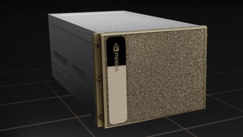
As with the A100, Hopper will initially be available on DGX H100 servers. Each DGX H100 system contains eight H100 GPUs, providing up to 32 PFLOPS of AI compute and 0.5 PFLOPS of FP64, with 640GB of HBM3 memory. The DGX H100 also has 3.6TB/s of bandwidth.
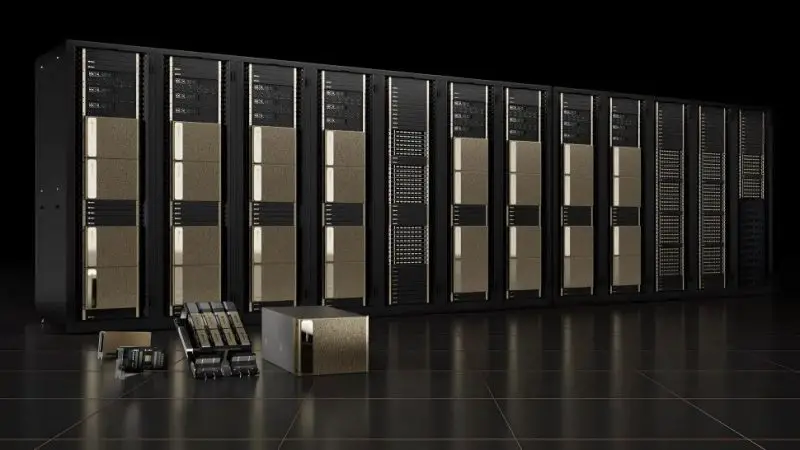
EOS supercomputer, equipped with the new DGX H100
Using multiple DGX H100 servers, Nvidia expands to a DGX SuperPod with 32 DGX H100 systems, linked to an upgraded NVLink Switch system and Quantum-2 InfiniBand network. A single SuperPod H100 features 256 H100 GPUs, 20TB of HBM3 memory, and up to 1 ExaFLOPS of AI compute, while delivering 70.4TB/s of bandwidth.
Of course, supercomputers can be built using multiple SuperPods, and Nvidia has announced its new Eos supercomputer that follows in Selene’s footsteps. The Eos will be built from 18 H100 SuperPods, with 576 DGX H100 systems and 360 NVLink switches, and will provide 275 PFLOPS of FP64 compute.
Related posts:
 7-nanometer Nvidia GPU, TSMC will handle most of the production
  ASRock X299, a new BIOS allows you to install 2 TB of memory
  MSI Prestige X570 Creation Review: Test | Specs | Hashrate
  Radeon RX 5500 XT, PCI Express 3.0 castrates performance?
  An overclocker ran 1TB of RAM on an X299 motherboard limited to 256GB
  Best Review 2021: MSI MPG X570 Gaming Edge WiFi Under $250 ($200)