In the summer of 2008, AMD launched the Radeon HD 4870 – the world’s first graphics card with GDDR5 memory. The memory standard entailed a significant bandwidth increase compared to aging GDDR3 and has since its introduction been developed to offer ever higher clock frequencies and thus also bandwidth.
The latest news about GDDR5 is that SK Hynix has achieved a breakthrough by offering capsules with the standard frequency 2,000 MHz (8,000 MHz efficient). However, this does not come without disadvantages in the form of increased power consumption, where memory makes an increasing claim as AMD and Nvidia push the boundaries.
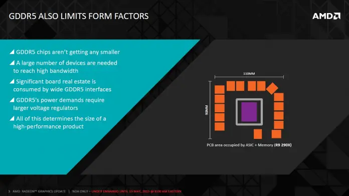
Another disadvantage that applies to GDDR5, but also representatives such as GDDR3, is that the separate memory capsules do not become smaller and that many are needed to reach the high bandwidth required. For example, the graphics processor Hawaii in the Radeon R9 290X is surrounded by no less than 16 GDDR5 capsules, something that has a direct impact on the ability to shrink the physical size of the graphics card.
Historically, integration of components on the same silicon as the processor has solved similar concerns, but memory in particular is too cost-effective. Here comes HBM – High Bandwidth Memory – into the picture and once again, AMD is the first to take advantage of a new memory technology.

The concept differs markedly from previous solutions. Instead of mounting the memory on the circuit board (graphics card), the capsules are placed close to the graphics processor via a so-called interposer or “intermediate storage”. This is as close as possible to integrating two components without belonging to the same circuit.
Before the advantages, the solution is drawn with a disadvantage. The intermediate layer is in itself a piece of silicon with pipelines, something that raises the price and at least in the short term means that the technology is not suitable for price-pressed solutions. In addition to this, however, the advantages are many compared to today’s GDDR5.
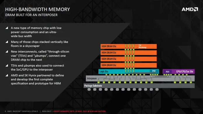
AMD emphasizes that the close integration makes it possible to use a very simple memory controller with considerably less noise-reducing logic than before. This in turn leads to more space being freed up for more powerful processors with more computing units and higher clock frequencies.

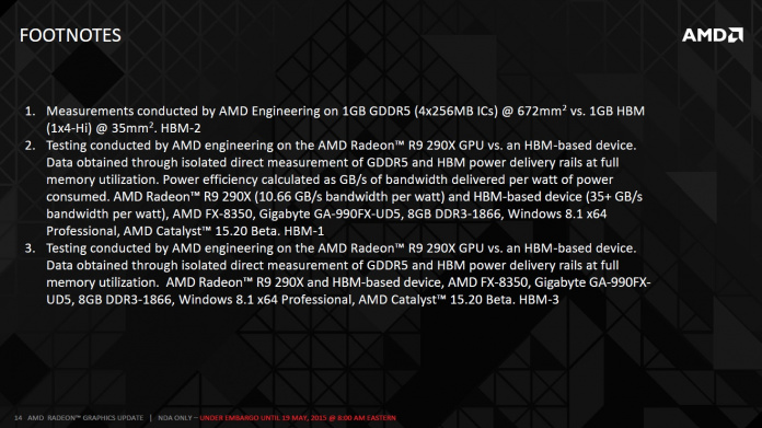
The memory technology will also drastically reduce the power consumption against GDDR5, which in AMD’s tests delivers 10.66 GB / s per consumed watt with a Radeon R9 290X, which has a memory bandwidth of 320 GB / s. In other words, the memory accounts for 30 watts of the graphics card’s total power consumption, and it does not count on the graphics processor’s memory controls. Compared to an as yet unspecified HBM-based solution, energy efficiency increases several times to offer at least 35 GB / s per consumed watt.
The basis of the technology is stacked memory according to the concept through-silicon via (TSV), where the memory circuits are produced with physical holes filled with conductive materials. This creates vertical lead paths when the circuits are joined. The advantage is that lower voltage is required to send signals between the circuits, which results in lower power consumption and thus more room for higher performance.
The pictures show that the HBM memory is considerably higher than the processor, something that could make cooling difficult. However, it is important to take the presentation pictures for what they are – illustrations. AMD’s Joe Macri explains that the wafer for the memory circuits measures in at a few hundred micrometers in thickness, which means that the end product is not very high.
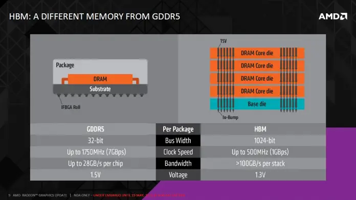
In the first generation HBM, called HBM1, four circuits are stacked on top of each other. Each has two 128-bit IO connectors, for a massive bus width of 1,024 bits per memory capsule. This includes the voltage 1.3 V and a clock frequency of 500 MHz (1,000 MHz efficient), for a bandwidth of 128 GB / s. In AMD’s own illustrations, the processor is accompanied by four HBM capsules, which corresponds to 512 GB / s via an ultra-wide 4,096-bit memory bus.
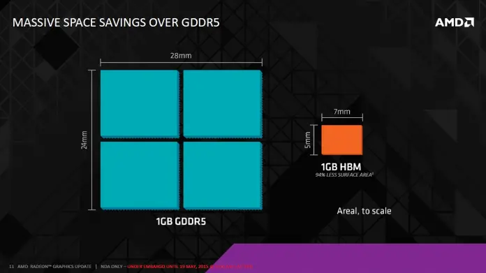
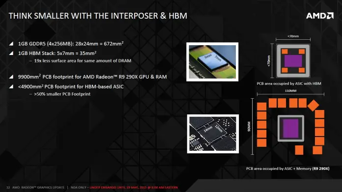
The last problem HBM solves is that previous technologies such as GDDR5 take up a lot of space physically. Each capsule offers the same amount of video memory as four GDDR5 memory capsules, while each HBM module is smaller. For AMD’s as yet unspecified HBM-based product, this means a halving in space for graphics processor and memory compared to the Radeon R9 290X, something that at least on paper guarantees smaller graphics cards even in the highest performance segment.
AMD does not want to go into any further details about the upcoming product with HBM, but only reveals that it is a graphics card. However, the memory technology is not exclusive to that type of product, but can also be used in, for example, more lavish APU circuits with integrated graphics in the upper middle segment.
Related posts:
 Review & Test: Video card Gigabyte GeForce RTX 3060 Ti Gaming OC Pro
  AMD Radeon RX 5600 XT VS GTX 1660 Ti and RTX 2060: Review| Set-up| Hashrate
  Review of the KFA2 GeForce RTX 3060 Ti Core video card
  GIGABYTE GeForce RTX 3090 Gaming OC video card: Review| Specs | Set-up|
  INNO3D GeForce RTX 3090 iCHILL X4 video card review: Test | Config | Hashrate
  ROG Strix GeForce RTX 3070 OC Review: Test | Specs | Hashrate