In early December 2016, SweClockers, together with other media, took part in AMD’s plans for 2017. In addition to the long-awaited architecture Zen, the company gave a first review of the graphics architecture Vega, which will give Nvidia a much-needed match in the performance segment.
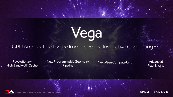
Since the introduction of the Tahiti graphics circuit that formed the basis of the Radeon HD 7970, AMD has used the Graphics Core Next (GCN) architecture, where the company to date with Polaris has made minor changes. Vega will be another development, but this is not about a new generation GCN.
With Vega, AMD is laying a new foundation Next-Generation Compute Unit or NCU, which in many ways differs greatly from GCN. The first major change is a brand new memory controller called High-Bandwidth Cache Controller (HBCC), which will fix what AMD thinks is the big problem with today’s graphics chips.
New manufacturing technologies allow AMD and Nvidia to accommodate more transistors and thereby achieve higher performance. While computing power increases sharply for each new generation, the same amount of memory does not apply, which primarily creates problems in various professional applications.
HBCC is intended to be compatible with virtually any type of memory, from GDDR5 to HBM, SSDs and even system memory. One of the highlights is that it supports up to 512 TB of virtual memory, something that opens up completely new possibilities when, for example, rendering photorealistic scenes.
Another news is Adaptive, fine-grained data movement, which will make the use of graphics memory more efficient. According to AMD, more than half of all memory is “wasted” in well-optimized game titles and even more in others. With the help of the new technology, this will be made more efficient, which should mean that a certain amount of memory will last longer than before. As an example, AMD takes a scene from Deus Ex: Mankind Divided where as many as 220 million polygons are rendered. Of these, the player sees only about 2 million or just under a hundredth.
The second novelty is a new unit for geometry calculations, which will deliver over twice as much performance per clock frequency. An important part of this is that the NCU supports Primitive shaders, something AMD in the long run thinks will replace Vertex and Geometry shaders. However, game developers must choose to embrace this type of shaders in their game engines, so it will probably be some time before this could be a potential benefit for AMD.
The next part is the calculation unit itself, NCU, which is much more flexible than GCN. In addition to support for single-precision (32-bit) calculations, there is also support for 16-bit and 8-bit calculations, which doubles and quadruples the theoretical computing power in applications and games that benefit from this.
Furthermore, AMD says that NCU has been optimized to deliver more instructions per clock cycle (IPC) and has been optimized for high clock frequencies. Taken together, this should mean real performance increases, even if previous rumors that Vega “only” has 4,096 stream processors, the same as Fiji in the Radeon R9 Fury X, are true.
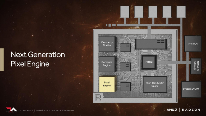
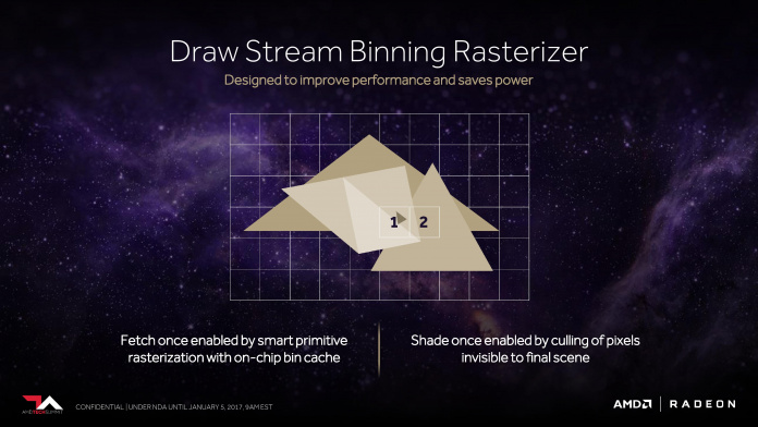
The fourth big news AMD highlights with Vega is called Next Generation Pixel Engine with Draw Stream Binning Rasterizer, which will deliver higher performance than before and at the same time help to reduce power consumption. The function is very reminiscent of Tile-Based Rasterization, which has long been used by mobile system circuits but also Nvidia’s architectures Maxwell and Pascal.
No product details
During the event, AMD was clear that they do not yet intend to reveal any “product details”. How an NCU is structured, how many stream processors Vega will get and not least the amount of memory were things they chose to put the lid on. However, Radeon CEO Raja Koduri showed the Vega 10 graphics circuit on stage and it was clear that it is accompanied by two HBM2 memory capsules.
A test system was also shown on site with a very early copy of Vega that ran around the game Doom. In this it was found that the amount of memory is 8 GB, which means that each HBM2 capsule has a capacity of 4 GB. Each capsule is expected to be clocked at 1,000 MHz (2,000 MHz efficient), which over a memory bus of a total of 2,048 bits would provide a bandwidth of 512 GB / s.
Furthermore, a report some time ago says that Vega 10 will be equipped with 4,096 stream processors. When AMD announced the Radeon Instinct during the same event, it appeared that the Vega-based graphics card in the series will receive 25 TFLOPS in performance, however, this in calculations in semi-precision. Provided that the information on the number of stream processors is correct, this means that AMD aims for Vega to reach a clock frequency of at least 1,500 MHz.
The company also omits an exact launch date for Vega, but is content to relay the first half of 2017. By all accounts, it will be later in that period, closer to the summer months.
Related posts:
 Review & Test: Video card Gigabyte GeForce RTX 3060 Ti Gaming OC Pro
  AMD Radeon RX 5600 XT VS GTX 1660 Ti and RTX 2060: Review| Set-up| Hashrate
  Review of the KFA2 GeForce RTX 3060 Ti Core video card
  GIGABYTE GeForce RTX 3090 Gaming OC video card: Review| Specs | Set-up|
  INNO3D GeForce RTX 3090 iCHILL X4 video card review: Test | Config | Hashrate
  ROG Strix GeForce RTX 3070 OC Review: Test | Specs | Hashrate