Earlier this summer, AMD launched the Vega architecture for professional use and was followed up in mid-August with the Radeon RX Vega 64 and RX Vega 56 for consumers. What they all have in common is that they are based on the Vega 10 circle, which is only the first member of the Vega family.
Where Vega 10 is aimed at the performance segment, Vega 11 is intended for the middle segment, and is expected to replace the Polaris 20 graphics circuit in the Radeon RX 580 and RX 570. Now the industry magazine Digitimes reports that Globalfoundries is responsible for the production of Vega 11, which is expected to go into production soon. .
Production will continue to take place on Globalfoundrie’s 14-nanometer technology and, like Vega 10, Vega 11 will also use the HBM2 memory technology, which is integrated close to the graphics circuit on a substrate. However, this process is not handled by AMD or Globalfoundries, but by a third party.
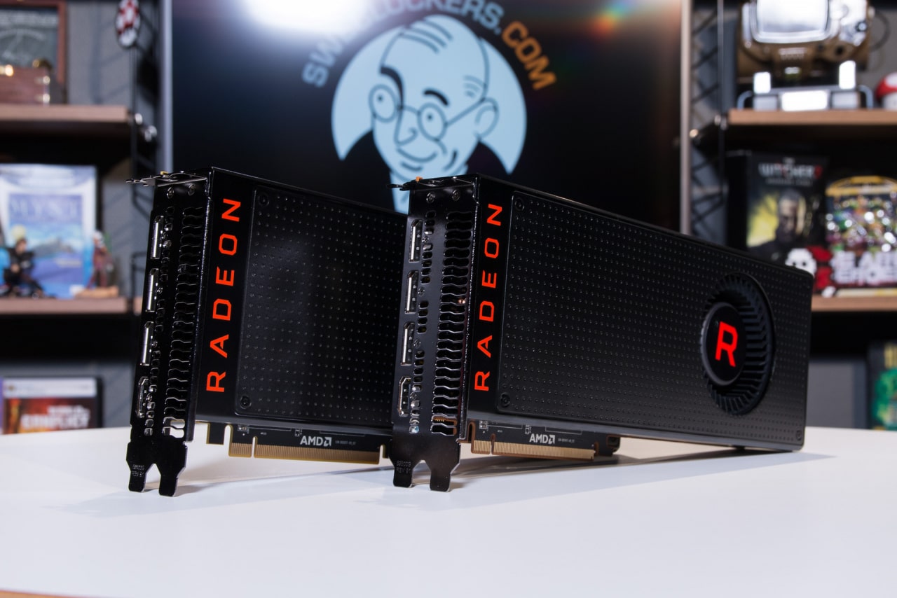
AMD Vega 10 (large circuit) with two HBM2 circuits in SweClocker’s test lab
Difficulties with integration should be one of the reasons for the low availability of graphics cards based on Vega 10, where AMD has chosen to turn to several partners. Here, Advanced Semiconductor Engineering (ASE) should have problems in its process, which is why AMD with Vega 11 is largely said to take the help of Siliconware Precision Industries (SLIP) for this part of the production.
AMD’s graphics circuit Vega 11 with associated graphics card is expected to be launched sometime later in 2017.
AMD Vega 20 at 7 nanometers
So far, AMD has not spoken officially about Vega 20, but recurring reports claim that such a graphics circuit is in the plans. Overall, the circuit is believed to have the same number of stream processors as Vega 10, 4,096, but with a doubled memory bus for a bandwidth of 1 TB / s and a new manufacturing technology for better energy efficiency.
For both Polaris and Vega, AMD has leased production to Globalfoundries at 14 nanometers, but for Vega 20 they will instead turn to 7 nanometers at TSMC. One reason for this is that TSMC has the ability to handle both the manufacture of the graphics circuit and handle the integration with a service they call Chip-on-Wafer-on-Substrate (CoWoS), something that can be thought to provide higher yield.
Related posts:
 Review & Test: Video card Gigabyte GeForce RTX 3060 Ti Gaming OC Pro
  AMD Radeon RX 5600 XT VS GTX 1660 Ti and RTX 2060: Review| Set-up| Hashrate
  Review of the KFA2 GeForce RTX 3060 Ti Core video card
  GIGABYTE GeForce RTX 3090 Gaming OC video card: Review| Specs | Set-up|
  INNO3D GeForce RTX 3090 iCHILL X4 video card review: Test | Config | Hashrate
  ROG Strix GeForce RTX 3070 OC Review: Test | Specs | Hashrate