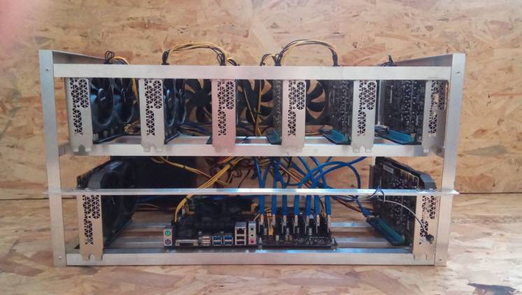
How to ‘Increase/Max/ Optimze/ Tune/ Boost’ Tesla A100 PCIe 40GB + 80GB Mining: Overlocking/ Hashrate/ Best Settings/ Specification – Nvidia Tesla A100 PCIe 40GB + 80GB Hashrate Consumption and Earnings
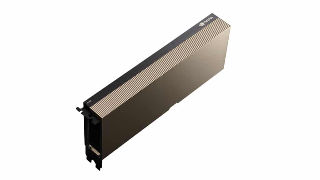
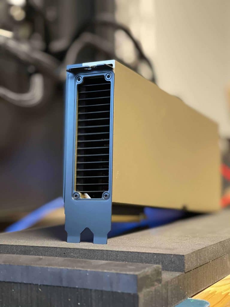
The 40GB Nvidia Tesla A100 is a Data Center and AI Training GPU released in June 2021. It features 40GB of HBM2e VRAM and is one of the most powerful GPUs ever produced to date. The peculiarity of this Video Card is given by the absence of an output for the video output. Despite this, it is capable of developing 170 mh / s without any Overclocking.
How to Increase Tesla A100 PCIe 40GB: Specifications
| CUDA Colors | 6912 |
| Transistor | 54.2 billion |
| GPU Clock (base) | 765 Mhz |
| GPU Clock (Boost) | 1410 Mhz |
| Dimensioni VRAM | 40 GB |
| VRAM model | HBM2e |
| VRAM speed | 1215 Mhz – 2,4 Gbps |
| Tensor Colors | 432 |
| Bus interface | PCIe 4.0 x16 |
| Bandwidth | 1555 GB/s |
| Memory Bus | 5120 bit |
| Consumption | 250w |
How to Maximize: Hashrate
The 40GB A100 is certainly a mind-boggling GPU, as is its purchase price: € 11,000. The price itself is an average, you can find it at lower or higher prices, but it remains a GPU for professional use and certainly not designed for mining. Despite this, this GPU is capable of pulling out excellent numbers: 170 mh / s at a consumption of 235w.
Based on these results, the GPU will be able to produce an impressive 170 mh / s at an average consumption of 235w. It will be able to produce up to € 8.05 per day and it will take around 1367 days of mining to pay off the purchase cost!
NVIDIA unveiled the NVIDIA A100 80GB GPU for the NVIDIA HGX AI supercomputing platform, with twice the memory of its predecessor, and designed to provide researchers and engineers with unprecedented speed and performance in their research in artificial intelligence and science.

The new A100 processor with HBM2e technology offers double the high-speed memory of up to 80GB compared to the A100 40GB and delivers more than 2 terabytes of bandwidth per second. This enables fast data transfers to the A100 GPU and further accelerates applications and leverages even larger models and datasets.
The 80GB model A100 is designed for a wide variety of memory-intensive applications:
- The A100 80GB delivers up to 3x acceleration for AI training in recommender models such as DLRM with spreadsheets representing billions of users and billions of products.
- Allows you to train the largest models with a large number of parameters suitable for a single HGX-based server such as GPT-2, eliminating the need for parallel data architectures or models that can be time-consuming to build and slow across multiple nodes.
- Thanks to MIG (multi-instance GPU) technology, the A100 can be split into instances, up to seven, each with 10GB of memory. This provides secure hardware isolation and maximizes GPU utilization for many small workloads.
- For inference to automatic speech recognition models such as RNN-T, a single MIG A100 80GB instance can handle much larger batch sizes, delivering 1.25x faster inference at work.
- In the retail big data analytics benchmark, the A100 80GB terabyte range improves performance up to 2x.
- Provides tremendous acceleration in scientific applications such as weather forecasting and quantum chemistry.
How to Optimize: Key features of A100 80GB
- Tensor cores of the third generation : up to 20 times faster in AI compared to the previous generation Volta with the new TF32 format, as well as 2.5 times faster in FP64 calculations for HPC, 20 times faster in INT8 calculations for inference, and support for BF16 format.
- Bigger and faster HBM2e memory : Double the memory bandwidth and, for the first time in the industry, more than 2 TB / s bandwidth.
- MIG technology : Doubling memory per isolated instance, up to seven MIG systems with 10GB of memory each.
- Structural Sparsity : Up to 2x speedup in inference of sparse models.
- NVLink and 3rd Generation NVSwitch : Doubling the bandwidth between GPUs over previous communication technology accelerates data transfers to GPUs for demanding tasks up to 600 GB / s.
NiceHash managed to get their hands on an NVIDIA A100 40GB and did some tests. They managed to achieve a whopping 171 MH/s at 210 Watt of electricity usage.
All you have to do is disable ECC (Error Correction Code). Disabling it will increase speed or lower consumption from 250W to 210W.
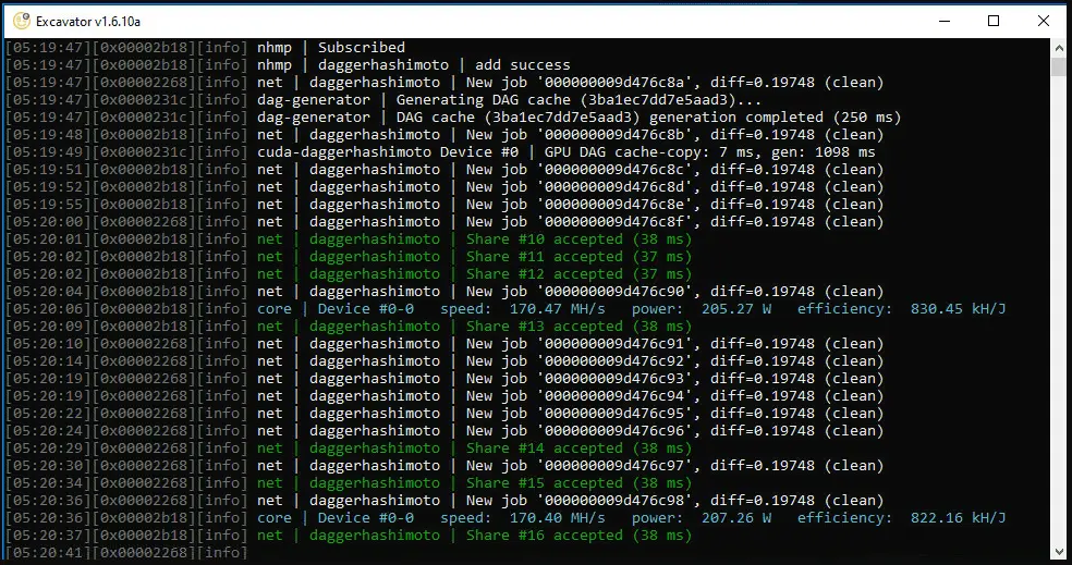
NVIDIA TESLA A100 PCIE 40GB mining hashrate for each algorithm : [ Power Consumption 200 Watts/Hour ] :
DaggerHashimoto [ EtHash : (ETH) & (ETC) ] Ethereum Mining Hashrate : 170 MH/s
How to Increase Tesla A100 PCIe 40GB + 80GB: NVIDIA Accelerator Specification Comparison
| NVIDIA Accelerator Specification Comparison | ||||
| 80GB A100 (PCIe) | 80GB A100 (SXM4) | 40GB A100 (PCIe) | 40GB A100 (SXM4) | |
| FP32 CUDA Cores | 6912 | 6912 | 6912 | 6912 |
| Boost Clock | 1.41GHz | 1.41GHz | 1.41GHz | 1.41GHz |
| Memory Clock | 3.0 Gbps HBM2 | 3.2 Gbps HBM2 | 2.43Gbps HBM2 | 2.43Gbps HBM2 |
| Memory Bus Width | 5120-bit | 5120-bit | 5120-bit | 5120-bit |
| Memory Bandwidth | 1.9TB/sec (1935GB/sec) | 2.0TB/sec (2039GB/sec) | 1.6TB/sec (1555GB/sec) | 1.6TB/sec (1555GB/sec) |
| VRAM | 80GB | 80GB | 40GB | 40GB |
| Single Precision | 19.5 TFLOPs | 19.5 TFLOPs | 19.5 TFLOPs | 19.5 TFLOPs |
| Double Precision | 9.7 TFLOPs (1/2 FP32 rate) | 9.7 TFLOPs (1/2 FP32 rate) | 9.7 TFLOPs (1/2 FP32 rate) | 9.7 TFLOPs (1/2 FP32 rate) |
| INT8 Tensor | 624 TOPs | 624 TOPs | 624 TOPs | 624 TOPs |
| FP16 Tensor | 312 TFLOPs | 312 TFLOPs | 312 TFLOPs | 312 TFLOPs |
| TF32 Tensor | 156 TFLOPs | 156 TFLOPs | 156 TFLOPs | 156 TFLOPs |
| Relative Performance (SXM Version) | 90%? | 100% | 90% | 100% |
| Interconnect | NVLink 3 12 Links (600GB/sec) | NVLink 3 12 Links (600GB/sec) | NVLink 3 12 Links (600GB/sec) | NVLink 3 12 Links (600GB/sec) |
| GPU | GA100 (826mm2) | GA100 (826mm2) | GA100 (826mm2) | GA100 (826mm2) |
| Transistor Count | 54.2B | 54.2B | 54.2B | 54.2B |
| TDP | 300W | 400W | 250W | 400W |
| Manufacturing Process | TSMC 7N | TSMC 7N | TSMC 7N | TSMC 7N |
| Interface | PCIe 4.0 | SXM4 | PCIe 4.0 | SXM4 |
| Architecture | Ampere | Ampere | Ampere | Ampere |
At a high level, the 80GB upgrade to the PCIe A100 is pretty much identical to what NVIDIA did for the SXM version. The 80GB card’s GPU is being clocked identically to the 40GB card’s, and the resulting performance throughput claims are unchanged.
Related posts:
 How to overclock a graphics card in a laptop: MSI Afterburner – AMD & NVIDIA
  I7 4770K (OC) with RX 5700 XT: Hashate | |overclocking | Benchmark | 8 Games HD
  Red Dead Redemption 2: Overclocked FX 8350 and RX 5700 XT in FULL HD resolution
  AMD Radeon RX 6700 XT Mining: Hashrate | overclocking| Settings | Power Consumption
  How to increase: RTX 2060 vs 2060 Super Mining- Overclocking | HiveOS | Rave OS
  GTX 1080 Ti VS 1080 Mining: Overclocking | Profitability (Ether) | Power consumption