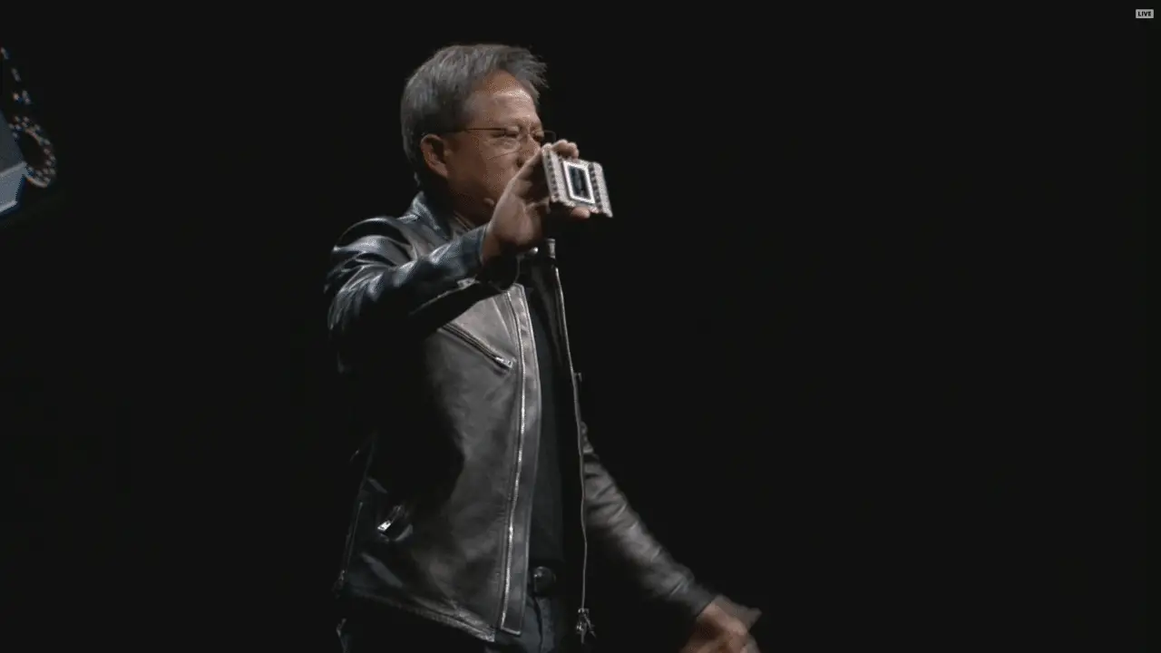
True to tradition, Nvidia holds its annual GPU Technology Conference and during a session, the company’s founder and CEO Jen-Hsun Huang always takes the stage. Last year, the architecture Pascal was achieved with the calculation card Tesla P100 and for the 2017 edition, it’s time for the next step – Time.
Specifications: Nvidia Tesla V100
Tesla V100 | Tesla P100 | Tesla M40 | Tesla K40 | |
|---|---|---|---|---|
Technical | 12nm TSMC | 16nm TSMC | 28nm TSMC | 28nm TSMC |
Circuit | GV100 | GP100 | GM200 | GK110 |
Circuit surface | 815 mm2 | 610 mm2 | 601 mm2 | 551 mm2 |
Transistors | 21.1 billion | 15.3 billion | 8 billion | 7.1 billion |
Architecture | Time | Pascal | Maxwell | Kepler |
SM cluster | 80 st. | 56 st. | 24 st. | 15 st. |
CUDA cores | 5 120 st. | 3 584 st. | 3 072 st. | 2 880 st. |
Texture units | 320 st. | 224 st. | 192 st. | 240 st. |
Clock frequency | 1 370 MHz | 1 328 MHz | 948 MHz | 745 MHz |
GPU Boost | 1 455 MHz | 1 480 MHz | 1 114 MHz | 875 MHz |
Calculating power (SP, FP32) | 14 899 GFLOPS | 10 608 GFLOPS | 6 844 GFLOPS | 5 040 GFLOPS |
Calculating power (DP, FP64) | 7 450 GLOPS | 5 304 GFLOPS | 214 GFLOPS | 1 680 GFLOPS |
Memory bus | 4 096-bit | 4 096-bit | 384-bit | 384-bit |
Minnestyp | HBM2 | HBM2 | GDDR5 | GDDR5 |
Memory amount | 16 GB | 16 GB | Up to 24 GB | Up to 12 GB |
Memory frequency | ~1 750 MHz | 1 430 MHz | 6 000 MHz | 6 000 MHz |
Memory bandwidth | 900 GB/s | 732 GB/s | 288 GB/s | 288 GB/s |
TDP | 300 W | 300 W | 250 W | 235 W |
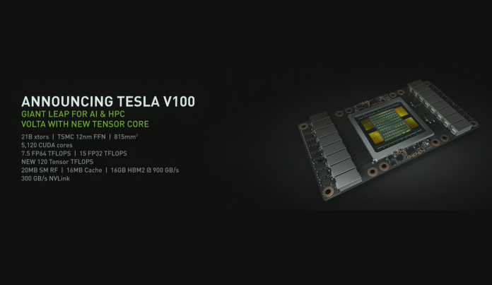
The new calculation card is called Tesla V100 and debuts the architecture Volta. The GV100 graphics circuit is based on TSMC’s 12-nanometer technology, which is based on last year’s 16 nanometers but with optimizations for energy efficiency, performance and transistor density. This enables Nvidia to create the most advanced and largest circuit ever.
► Read all articles about #Nvidia Volta
The graphics circuit houses no less than 21 billion transistors, which is comparable to 15.3 billion transistors for the previous GP100 record holder. This with a circuit area of massive 815 mm2, considerably larger than single circuits that have historically measured at most closer to 700 mm2.
The number of CUDA cores for the Tesla V100 is 5,120 and the computing power is stated to be 15 TFLOPS for single precision (FP32) and 7.5 TFLOPS for double precision (FP64). In addition to this, there is a new type of Tensor cores that can perform calculations specifically for machine learning and with these, the theoretical computing power is as much as 120 TFLOPS.
The solid graphics circuit is surrounded by four 4 GB HBM2 capsules each with a clock frequency of 875 MHz (1,750 MHz efficient), giving a total of 16 GB of memory and a theoretical bandwidth of 900 GB / s. In terms of connectivity, the Tesla V100 supports second-generation NVLink with a bandwidth of 300 GB / s – almost ten times higher than 32 GB / s for PCI Express 3.0 x16.
Deliveries of the Nvidia Tesla V100 will begin during the third quarter of the year. It is not clear when the new graphics circuit will be released to consumers, but with Pascal in mind, it is likely that Nvidia will create a smaller and more energy-efficient circuit called the GV102 without computationally oriented features.
Related posts:
 Review & Test: Video card Gigabyte GeForce RTX 3060 Ti Gaming OC Pro
  AMD Radeon RX 5600 XT VS GTX 1660 Ti and RTX 2060: Review| Set-up| Hashrate
  Review of the KFA2 GeForce RTX 3060 Ti Core video card
  GIGABYTE GeForce RTX 3090 Gaming OC video card: Review| Specs | Set-up|
  INNO3D GeForce RTX 3090 iCHILL X4 video card review: Test | Config | Hashrate
  ROG Strix GeForce RTX 3070 OC Review: Test | Specs | Hashrate