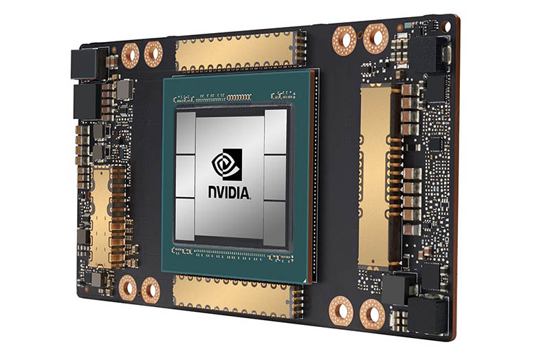
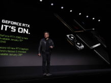
In an unusual advertisement from his kitchen, Jensen Huang officially presented his new architecture for GPUs and "Ampere" computing cards, along with the new Tesla A100, his first flagship product based on this architecture.
Designed to succeed the Volta-based Tesla V100, this new Tesla A100 has the same purpose as its predecessor: To deliver the highest possible performance in artificial intelligence that current technologies allow. These are some of its main characteristics:
- More than 54 billion transistors, being the largest 7nm manufactured processing unit in the world
- Third Generation Tensor Cores with TF32, a new mathematical format that accelerates single precision AI training, offering up to 20x more performance than FP32 without code changes. It also supports FP64, offering up to 2.5x more performance than Volta.
- Multiple GPU instances, or MIGs, allowing a single A100 to be partitioned into up to 7 independent GPUs, each with its own resources.
- NVLink 3rd Generation, doubling the high-speed connection between GPUs, allowing servers with A100 to act as a single giant GPU.
All this allows for 6x more performance than Volta in AI training, and 7x more performance in inference.
Unfortunately there is not much information on its specifications, although we know the following:
- 6912 Cuda Cores
- 40GB of VRAM HBM2e
- 1.55GB / s memory bandwidth
- NVLINK 3.0 support with bandwidth up to 600GB / s
- There will be versions with PCI-E form factor with PCI-E 4.0 interface
- 400W TDP
- Manufactured under the 7nm TSMC process
These new Tesla A100 GPUs will be available in the new DGX A100 system that we will talk about later, and also on different servers of Nvidia's partners, in addition to multiple supercomputers and cloud services from Microsoft, Google, Amazon, and more.
What do you think about the new Tesla A100 from Nvidia? Are you eager to see them in action?
Related posts:
 7-nanometer Nvidia GPU, TSMC will handle most of the production
  ASRock X299, a new BIOS allows you to install 2 TB of memory
  MSI Prestige X570 Creation Review: Test | Specs | Hashrate
  Radeon RX 5500 XT, PCI Express 3.0 castrates performance?
  An overclocker ran 1TB of RAM on an X299 motherboard limited to 256GB
  Best Review 2021: MSI MPG X570 Gaming Edge WiFi Under $250 ($200)