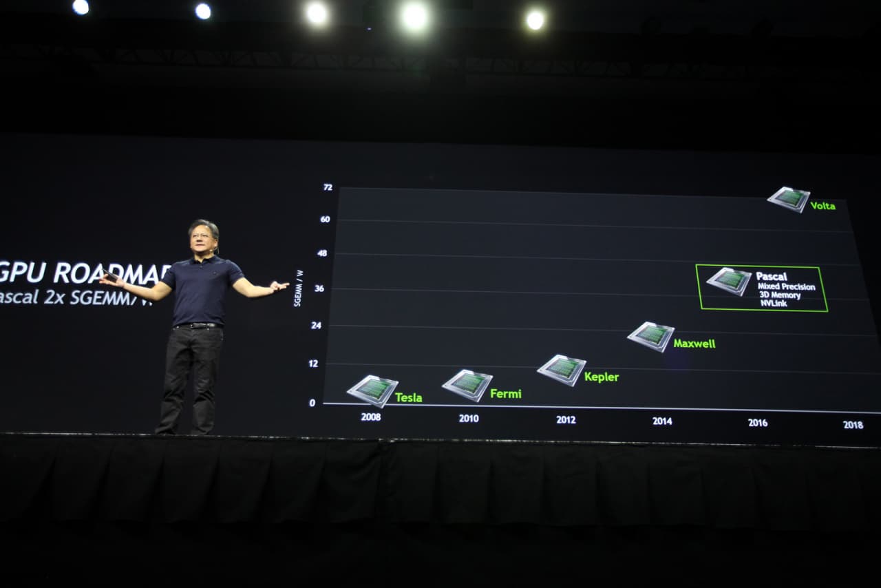
It will blow up to a storm in the graphics market in 2016. Next year, both Nvidia and AMD will go from 28 nanometers down to 16 or 14 nanometers at TSMC and Samsung and Globalfoundries respectively. With this, Nvidia is expected to follow AMD and take the step to the HBM memory standard, which will enable a bandwidth of 1 TB / s – double up from 512 GB / s for AMD’s graphics circuit Fiji.
Current for the second generation HBM, HBM2, is Nvidia’s successor to the GM200, which is believed to go by the code name GP100. However, a new monster circuit is not the only thing that is to be expected. Nvidia has at least one more graphics circuit underway, which according to new rumors will use a more cost-effective solution than HBM2.
3DCenter now reports that the GP104 intermediate circuit will use a further development of GDDR5 called GDDR5X. The big news is doubled prefetch, from 32 to 64 bytes of data at each memory access, which makes it possible to double the bandwidth up to regular GDDR5 memory.
At present, GDDR5 goes up to a maximum of 4,000 MHz (8,000 MHz efficiently), which together with a 256-bit memory bus provides 256 GB / s bandwidth. With GDDR5X, this could be doubled to 512 GB / s and thus be in line with AMD’s latest graphics cards Radeon R9 Fury X, R9 Fury and R9 Nano.
According to the same information, GDDR5X will be delayed until the end of 2016, which should probably mean the same for the GP104 intermediate circuit.
Related posts:
 Review & Test: Video card Gigabyte GeForce RTX 3060 Ti Gaming OC Pro
  AMD Radeon RX 5600 XT VS GTX 1660 Ti and RTX 2060: Review| Set-up| Hashrate
  Review of the KFA2 GeForce RTX 3060 Ti Core video card
 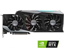 GIGABYTE GeForce RTX 3090 Gaming OC video card: Review| Specs | Set-up|
  INNO3D GeForce RTX 3090 iCHILL X4 video card review: Test | Config | Hashrate
 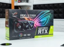 ROG Strix GeForce RTX 3070 OC Review: Test | Specs | Hashrate