Nvidia’s new graphics architecture Turing was launched in September 2018 as the cornerstone of the Geforce RTX family, where dedicated components for acceleration of ray tracing was architecture’s big parade number. Now the first concrete information is revealed about the architecture’s sequel Ampere, which will reach the market next year.
The information comes from Taiwan’s largest technology publication Digitimes, which in addition to the launch year also reveals that Nvidia is changing manufacturing partners. Graphics cards based on the Ampere architecture will be manufactured by Samsung on their improved 7-nanometer technology with EUV lithography.
Samsung’s production of 7 nanometers with EUV technology will provide 50 percent improved energy efficiency compared to the company’s 10-nanometer technology.
EUV stands for Extreme Ultra-violet Litography, an improved form of lithography where other wavelengths of light are used to facilitate the manufacture of circuits on such a small scale. The circuits will be easier to manufacture for Samsung, while their performance ratio has the potential to be as much as 50 percent better per watt compared to Samsung’s existing manufacturing technology of 10 nanometers.
At present, Nvidia together with rival AMD are two of TSMC’s largest customers of the company’s 7 nanometer UV technology. TSMC also has a manufacturing node based on EUV technology planned, but the reason for Nvidia’s change does not appear in Digitime’s report. It may be that Samsung offered a better deal, but it may also be because Samsung’s EUV solution has advantages over TSMC’s.
Another potential reason may be that Nvidia estimates that TSMC will not be able to offer sufficiently large quantities of circuits. In 2020, TSMC will continue to manufacture processors, graphics chips and integrated circuits for AMD as well as integrated circuit sets for most mobile phone manufacturers. Samsung has sufficient production capacity to cover Nvidia’s needs for Ampere.
In addition to Samsung’s 7 nanometer EUV technology, the company has presented milestones in the manufacture of circuits of 5 nanometers and 3 nanometers, which is rumored that Samsung can grow into an even bigger competitor to TSMC than they are today.
Source: Digitimes (via Wccftech)
Read more about Nvidia Ampere:
Related posts:
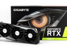 Review & Test: Video card Gigabyte GeForce RTX 3060 Ti Gaming OC Pro
 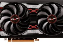 AMD Radeon RX 5600 XT VS GTX 1660 Ti and RTX 2060: Review| Set-up| Hashrate
 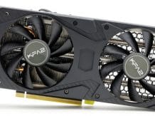 Review of the KFA2 GeForce RTX 3060 Ti Core video card
 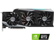 GIGABYTE GeForce RTX 3090 Gaming OC video card: Review| Specs | Set-up|
  INNO3D GeForce RTX 3090 iCHILL X4 video card review: Test | Config | Hashrate
  ROG Strix GeForce RTX 3070 OC Review: Test | Specs | Hashrate