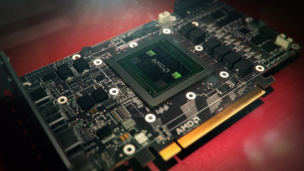
Since the introduction of the ATI Radeon HD 4870 in the summer of 2008, the GDDR5 memory technology has dominated graphics cards in the performance segment, to now be more or less standard regardless of price range. With the introduction of the Radeon R9 Fury X did High-Bandwidth Memory (HBM) entrance and lifted the bandwidth to new heights.
Although the technology has advantages such as potential for higher memory bandwidth and lower power consumption, high costs limit the impact. SK Hynix and Samsung want to change this with a price-squeezed variant, which is not quite as capable as HBM2 but is considerably faster than the original HBM.
The cost-effective version should be able to deliver around 200 GB / s bandwidth per capsule, which can be compared to 128 GB / s for HBM and 256 GB / s for HBM2. To squeeze the cost, the silicon must use fewer through-silicon via (TSV), the capsules should be placed on a simpler “interposer” and be without the circuit that handles communication with the stacked memory circuits. In addition, support for error correction code (ECC) disappears.
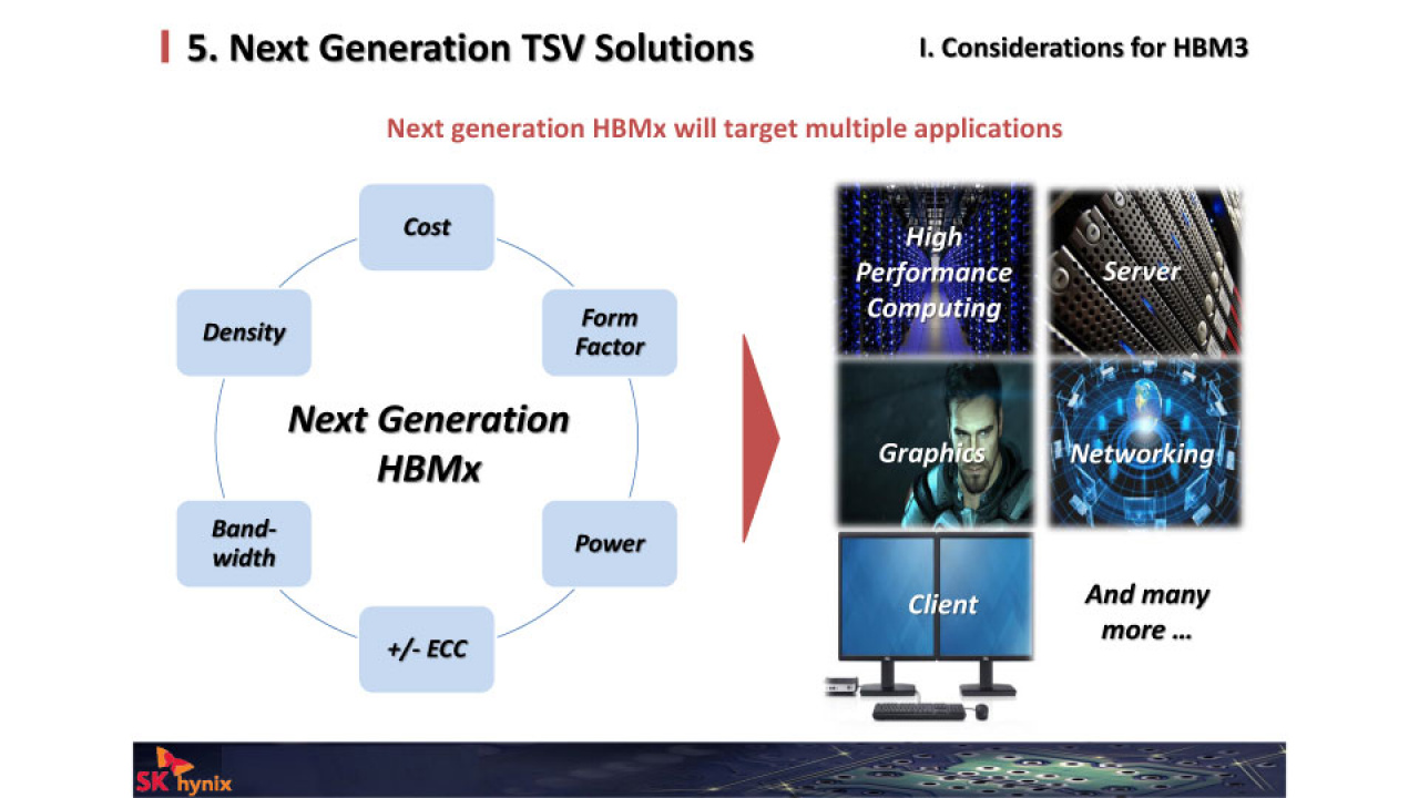
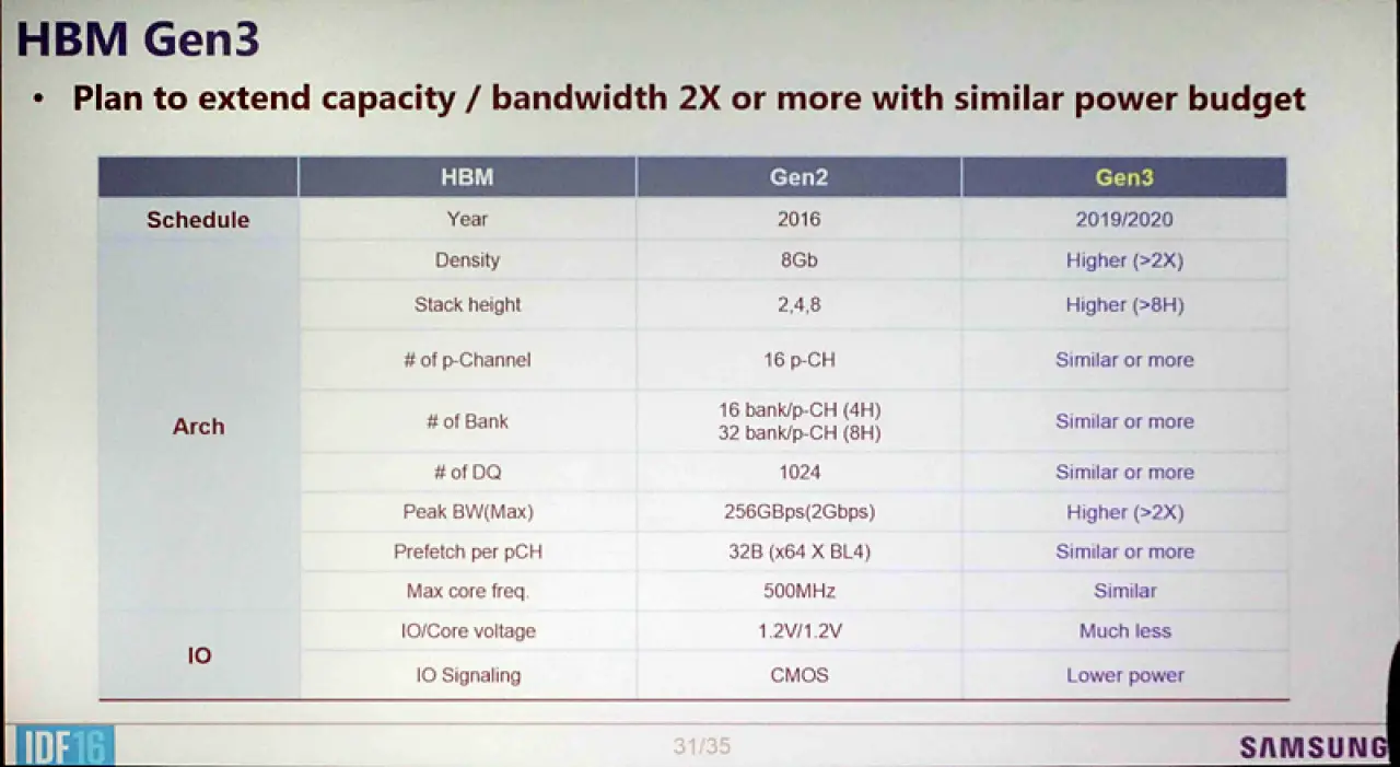
Later in the future, the next generation HBM – HBM3 is also planned. However, the technology is not expected to be completed until 2019–2020 and many details are thus not carved in stone. However, SK Hynix and Samsung aim to double both capacity and bandwidth, which would enable HBM3-based graphics cards to be delivered with 64 GB of graphics memory and a bandwidth of 2 TB / s.
Source: PC Watch.
Related posts:
 Review & Test: Video card Gigabyte GeForce RTX 3060 Ti Gaming OC Pro
 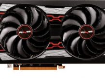 AMD Radeon RX 5600 XT VS GTX 1660 Ti and RTX 2060: Review| Set-up| Hashrate
 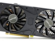 Review of the KFA2 GeForce RTX 3060 Ti Core video card
 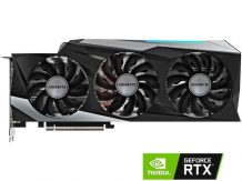 GIGABYTE GeForce RTX 3090 Gaming OC video card: Review| Specs | Set-up|
  INNO3D GeForce RTX 3090 iCHILL X4 video card review: Test | Config | Hashrate
  ROG Strix GeForce RTX 3070 OC Review: Test | Specs | Hashrate