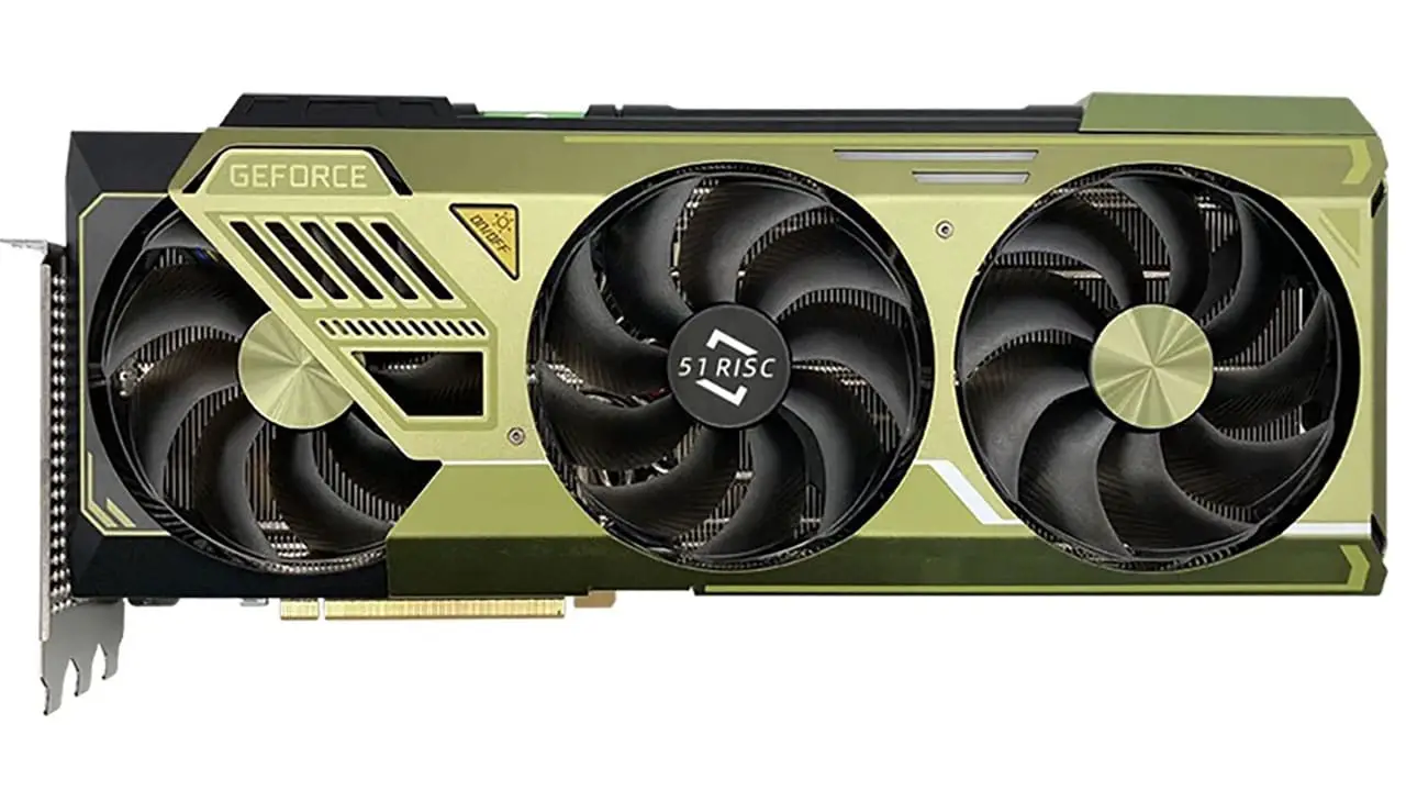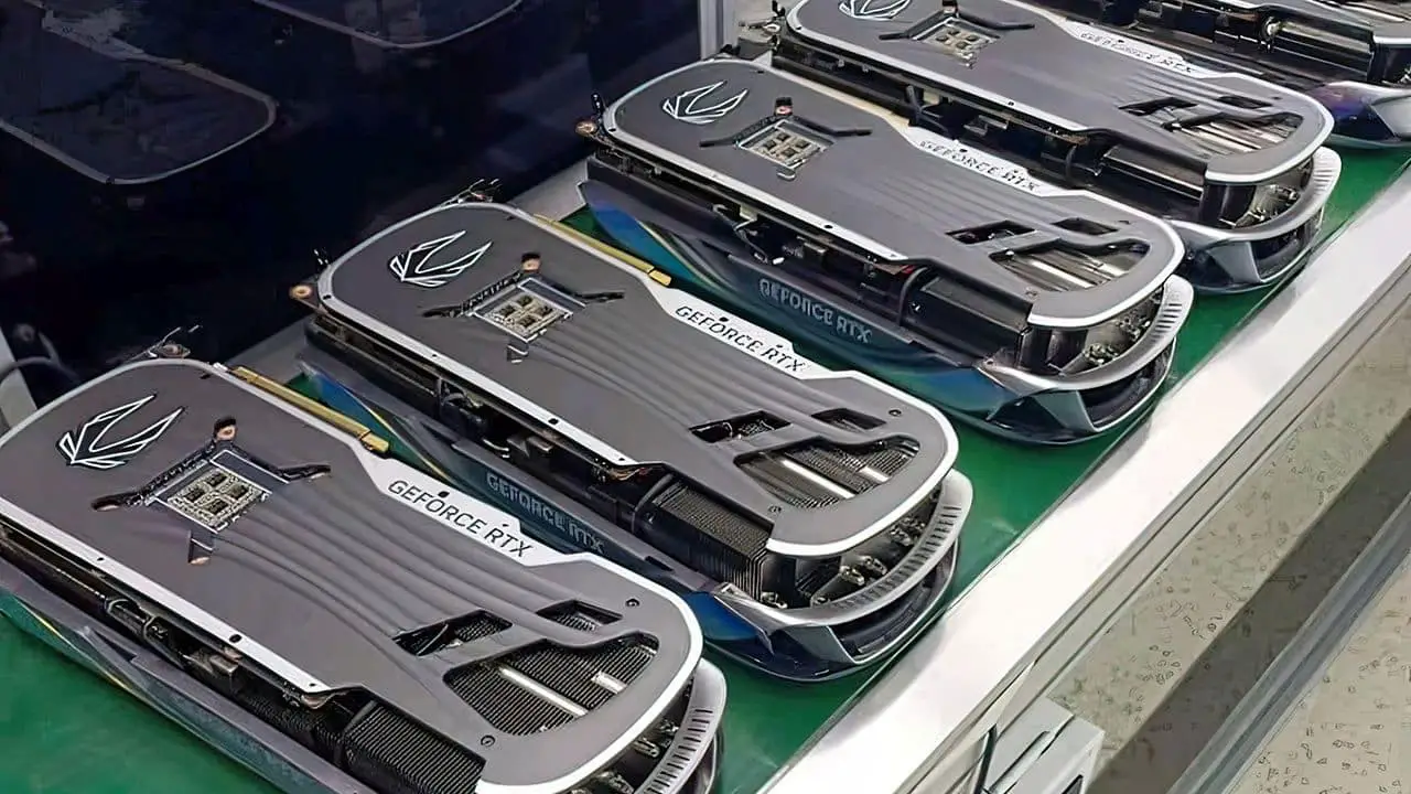
Asus TUF Gaming RTX 3080 OC |Specs | Price – After the arrival of ray tracing and DLSS at Nvidia and its first RTX Turing released in 2018, the founder is back on the attack with Ampere, an architecture that promises a big increase in performance for a price that does not skyrocket compared to the previous generation.
Indeed, while the MSRP of the RTX 2080 Super (and RTX 2080 before it) excluding FE was € 745, the new RTX 3080 are supposed to start at € 719. For our file, we recovered an Asus TUF Gaming RTX 3080 OC partner card, a model advertised at € 789. What does the beast have in its belly? This is what we will see!
Ampere
First of all and first change compared to Turing, the engraving fineness goes from 12 nm (TSMC) to 8 nm (Samsung). This allows the chips to be either smaller for an identical number of transistors, or on the contrary with more transistors of equal size, or even both at the same time! This is exactly the case for the GA102 which equips the RTX 3080 and 3090, the largest consumer DIE at present.
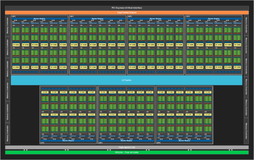
With a DIE of 628 mm² for 28.3 billion transistors, it is a large model but which remains smaller than the 754 mm² (and 18.6 billion transistors) for the TU102 which equips the RTX 2080 Ti. As for the RTX 2080 Super that the RTX 3080 replaces, the TU104 peaked at 545 mm² for “only” 13.6 billion transistors. There is therefore a big improvement in the density of the components. As can be seen from the diagram above, the GA102 has a total of seven GPCs, compared to six for Turing and his TU102. A GPC (Graphics Processing Clusters) is a block which contains the SMs, RT cores, tensors, CUDA cores as well as quite recently the ROPs, we can roughly compare it to a core found in desktop CPUs.
GA102 not yet complete
| RTX 2080 | RTX 2080 Super | RTX 2080 Ti | RTX 3080 | RTX 3090 | |
| GPU | TU104 | TU104 | TU102 | GA102 | GA102 |
| Engraving fineness | 12 nm | 12 nm | 12 nm | 8 nm | 8 nm |
| Number of transistors | 13.6 billion | 13.6 billion | 18.6 billion | 28.3 billion | 28.3 billion |
| DIE size | 545 mm² | 545 mm² | 754 mm² | 628 mm² | 628 mm² |
| SMs | 46 | 48 | 68 | 68 | 82 |
| CUDA hearts | 2944 | 3072 | 4352 | 8704 | 10496 |
| Cœurs Tensor | 368 | 384 | 544 | 272 | 328 |
| RT hearts | 46 | 48 | 68 | 68 | 82 |
| Base frequency | 1515 MHz | 1650 MHz | 1350 MHz | 1440 MHz | 1395 MHz |
| Boost frequency | 1710 MHz | 1815 MHz | 1545 MHz | 1710 MHz | 1695 MHz |
| Memory quantity | 8 Go GDDR6 | 8 Go GDDR6 | 11 Go GDDR6 | 10 Go GDDR6X | 24 Go GDDR6X |
| Memory frequency | 1750 MHz (14 Gbps) | 1937 MHz (15,5 Gbps) | 1750 MHz (14 Gbps) | 1188 MHz (19 Gbps) | 1219 MHz (19,5 Gbps) |
| Memory interface | 256 bits | 256 bits | 352 bits | 320 bits | 384 bits |
| TGP | 215 Watts | 250 Watts | 250 Watts | 320 Watts | 350 Watts |
Theoretically, this allows the GA102 to have 84 SM for just as many RT cores (for ray tracing management), but none of the GPUs on the market is equipped with this fully unlocked GA102. Even the RTX 3090, which is nevertheless the flagship of green, only accommodates 82 SM. Likewise, the GA102 of the RTX 3080 is even more castrated because it only has 68 SM, which is the equivalent of the old RTX 2080 Ti. If Nvidia does with Ampere what it did with Turing, it is easy to see Super or Ti variants arriving between the RTX 3080 and 3090, or even a more powerful model than the latter using a full GA102. But only time will tell!
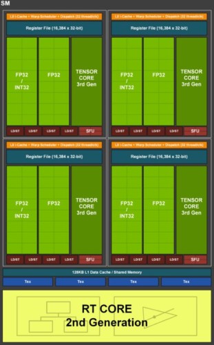
But looking at the technical characteristics, we see that despite the identical number of SMs between the RTX 2080 Ti and RTX 3080, Nvidia announces twice as many CUDA cores. How is it possible ? The founder doubled the number of FP32 units in each SM to do this. Indeed, when Turing had two distinct blocks, one dealing with integers (INT32) and the other with floating points (FP32), Ampere also offers two blocks with one dedicated to FP32 but the other allows both to process INT32 as well as the FP32. Turing introduced the ability to compute both INT32s and FP32s simultaneously using separate data paths. In this way, it is no longer necessary to calculate either an FP32 or an INT32. For Ampere, Nvidia wanted to take advantage of the dedicated INT32 data path (which is not nearly as used as that of the FP32s) in order to increase the potential raw power. To do this, he added 64 FP32 units (in addition to the 64 already present) but which share the path of the INT32s. Theoretically, therefore, and if the applications used only require floating point calculations, the raw power is doubled. If calculations on integers have to be done, it will be to the detriment of the FP32s on this data path. The given value of the CUDA cores therefore represents the best case scenario, when the GPU must only process FP32s. If the INT32 and FP32 units are loaded equally (and this is not won), we end up with an identical total of 4352 FP32 on the RTX 2080 Ti and 3080, or 5376 for a full GA102 against 4608 for a TU102 (Titan RTX) full.
RT and Tensor hearts
As with Turing, Ampere also has cores dedicated to processing ray tracing, or RT cores. Major argument during the release of the first RTX, Nvidia worked on this point for Ampere and brought a big boost to the performance level of each of these cores. After analyzing how its RT cores work in games, Nvidia saw that the main bottleneck was dealing with the intersections between different spokes and triangles. To remedy the problem, the throughput was doubled at this level. This does not mean that the performance is doubled, but the computing time is greatly improved, up to 70% depending on the founder.
Make way for GDDR6X
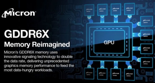
After introducing GDDR6 on its Turing generation, Nvidia is back in charge with the first GDDR6X chips! But that’s only true for the more high-end RTX 3080 and 3090 GPUs at the moment, the less capable models are content for now with GDDR6. Micron is at the origin of these new chips, the bandwidth is increasing sharply. Indeed, we go from GDDR6 14 Gbps chips on all RTX except the RTX 2080 Super (15.5 Gbps chips) to 19 Gbps for the RTX 3080 and 19.5 Gpbs for the RTX 3090. With a 320-bit bus for the RTX 3080 (760.3 Gb / s) is a good 53% of the available bandwidth compared to the RTX 2080 Super (495.9 Gb / s) against 23% for the RTX 2080 Ti (616 GB / s). But the GDDR6X modules are not yet pushed to their limits for the moment on the RTX 3000, there are modules capable of delivering 21 Gbps.
Increasing consumption
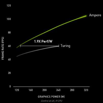
With characteristics so different between the “old” RTX 2080/2080 Super, namely more than double the transistors for an even bigger GPU, the maximum consumption increases. Indeed, we go from 215 (2080) and 250 Watts (2080 Super) to 320 Watts! We go beyond everything that has been presented so far at the level of consumer graphics cards. But if the noise level as well as the temperature do not explode as you could see on some GPUs in the past, it could be acceptable for this high end GPU. As much as it is necessary that the performances follow of course. If we are faced with a GPU consuming 320 Watts in the worst case and it is only 28% more efficient than another GPU consuming 250 Watts, we are not really facing a performance / consumption ratio. more interesting. According to Nvidia, this ratio would be 1.9X better on Ampere compared to Turing. But it’s not when the GPU is loaded to its maximum, we are talking about games clamped at 60 FPS (vertical sync) in both cases.
Related posts:
 7-nanometer Nvidia GPU, TSMC will handle most of the production
  ASRock X299, a new BIOS allows you to install 2 TB of memory
  MSI Prestige X570 Creation Review: Test | Specs | Hashrate
  Radeon RX 5500 XT, PCI Express 3.0 castrates performance?
  An overclocker ran 1TB of RAM on an X299 motherboard limited to 256GB
  Best Review 2021: MSI MPG X570 Gaming Edge WiFi Under $250 ($200)