
TSMC rushes the steps to first get to large-scale production of its 2nm process. The company in reported that it is moving forward with the development of next-generation nodes. The semiconductor giant it plans to put its first 3nm processes into production later this year and have 2nm ready by the end of 2025.
Bruce Lee, an analyst at Goldman Sachs, spoke to TSMC about inflation and the general economy, to which TSMC responded that it was well positioned, as the world’s leading smelter, to weather market fluctuations.
Another question was about the timeline for the 2nm node, to which the company replied: “Our N2 development is on track. We are confident that N2 will continue to provide technology leadership to support customer growth. And production will start in 2025,” said TSMC CEO CC Wei.
It is reported that N2 is the first TSMC process to use GAA (gate all-around) transistors instead of FinFETs (Fin Field Effect Transistors). Samsung has already started using its version of GAA and Intel wants to implement its version in 2024.

The interesting thing is that in the second half of this year, TSMC will put the N3 process into production. A year later, or possibly sooner, it will be ready to put into production the N3E process, which is a “performance and power” upgraded version of N3.
TSMC predicts that HPC (high performance computing) will be its fastest growing segment this year. Generated 41% of their revenue last quarter, only slightly more than smartphones, which generated 40%. IoT and automotive ranked third and fourth, generating 8% and 5% of revenue, respectively.
Total foundry revenue grew 11.6% quarter over quarter to $17.6 billion, slightly above its February guidance. Its second quarter revenue is expected to be between $17.6 billion and $18.2 billion for now.
Related posts:
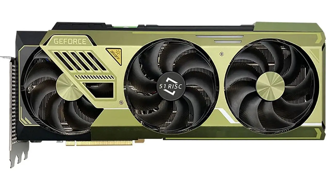
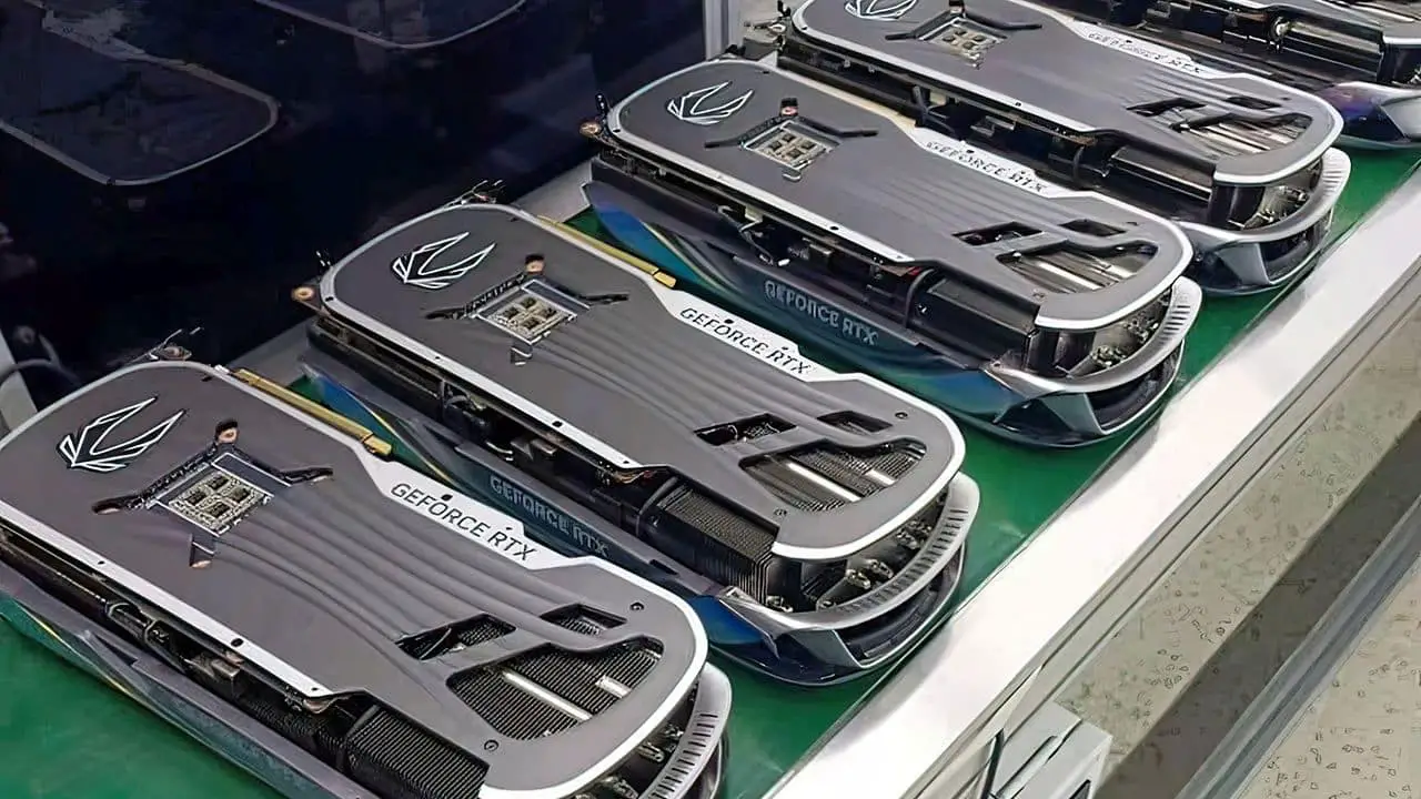
 7-nanometer Nvidia GPU, TSMC will handle most of the production
  ASRock X299, a new BIOS allows you to install 2 TB of memory
  MSI Prestige X570 Creation Review: Test | Specs | Hashrate
  Radeon RX 5500 XT, PCI Express 3.0 castrates performance?
  An overclocker ran 1TB of RAM on an X299 motherboard limited to 256GB
  Best Review 2021: MSI MPG X570 Gaming Edge WiFi Under $250 ($200)