Nvidia Ampere RTX-3000 technology in detail
: Test |CUP | Specs |Config
tl;dr: Nvidia has promised considerable increases in performance for the GeForce RTX 3090, 3080 and 3070. In the run-up to the test embargo, the manufacturer has now explained how the Ampere GPUs are supposed to do this and what the more than doubled number of shaders is all about. The FP32-ALUs are of great importance.
Where do shader and performance leaps come from?
The GA102-GPU offers an insane number of active ALUs on the new flagship GeForce RTX 3090. Nvidia names a whopping 10,496 CUDA cores and a theoretical computing power of 35.7 FP32 TFLOPS, which means a plus of 141 and 166 percent respectively compared to the GeForce RTX 2080 Ti – within one generation. And even the two smaller models still outshine the old top model. For a long time, the rumor mill talked about half of the shaders, and even press releases from board partners still contained them.
After initial explanations via Reddit, Nvidia has now also explained in a virtual Tech Day how Ampere’s streaming multiprocessors (SM) were converted to Turing in order to justify the number now specified and the TFLOPS derived from it. The basic structure of Ampere is identical to its predecessor, only a few details have changed – and they are crucial. Further changes affect the RT and the tensor cores, which are now also ready for 8K DLSS.
Ampere with serious changes in the SM
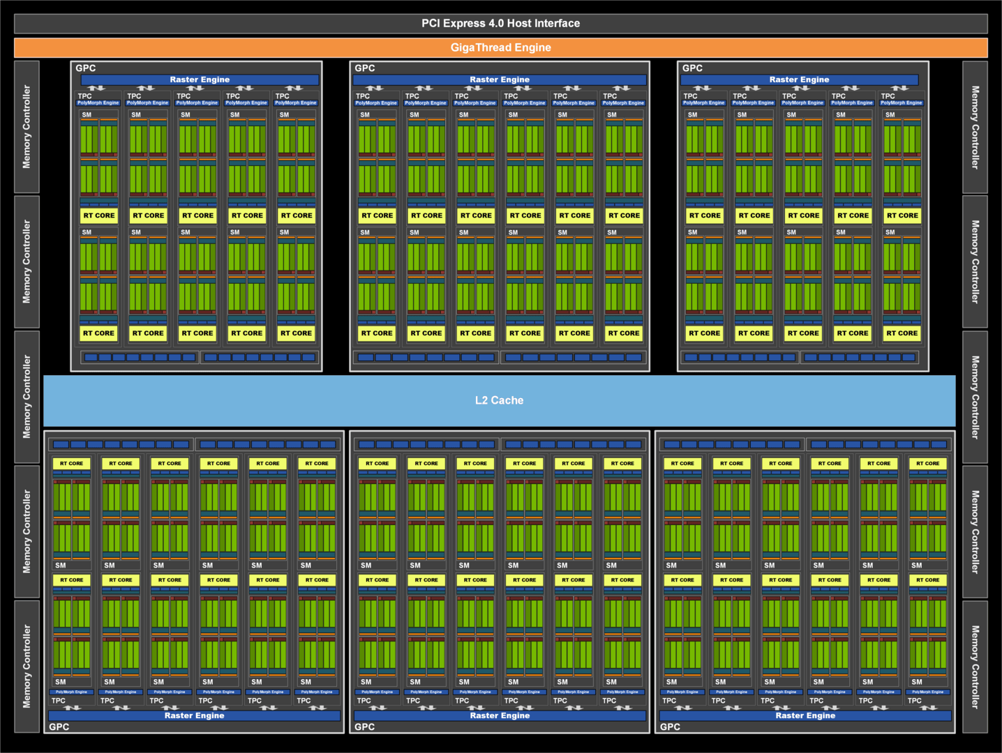
Nvidia has stuck to the basic structure: The GPU is still divided into several Graphics Processor Clusters (GPC), which contain the GPU’s arithmetic unit. This includes the Streaming Multiprocessors (SM) with the actual processing units, the Texture Processing Clusters (TPC) with the texture units, the geometry units for, for example, tessellation and, more recently, the ROPs.
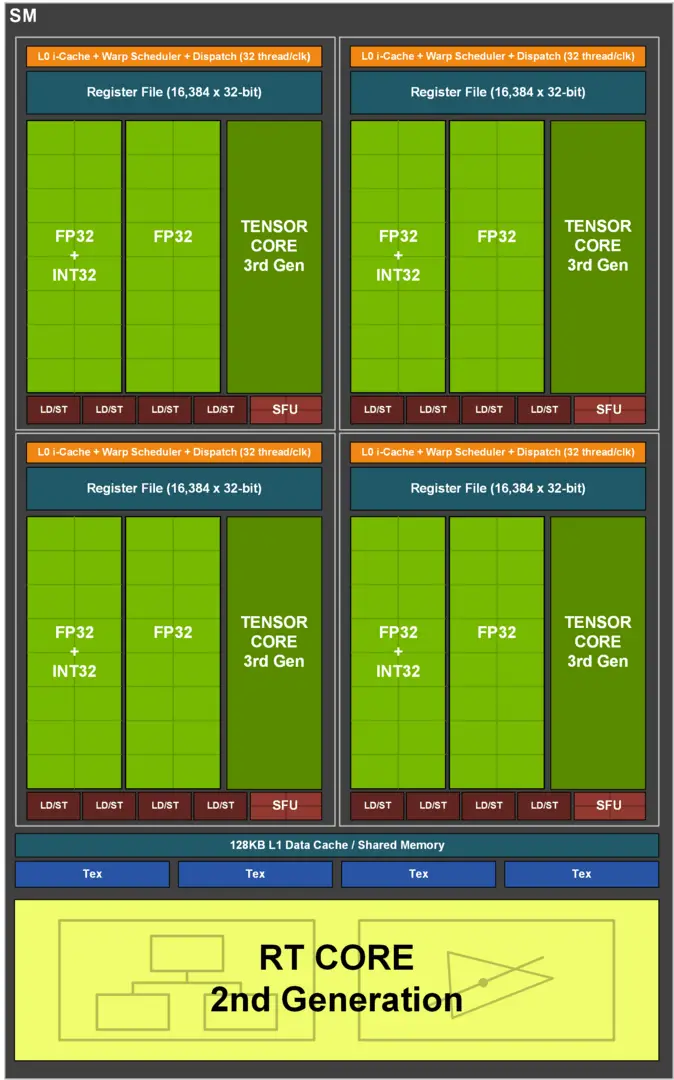
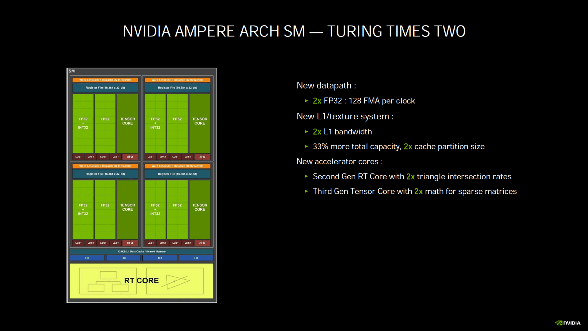
There have been serious changes within the framework. Ampere’s SM has been significantly upgraded compared to Turing’s. An SM at Turing is primarily composed of 64 FP32-ALUs for floating point calculations and 64 INT32-ALUs for integer calculations, which in turn are divided into four blocks of 16 FP32 and 16 INT32 ALUs each. The FP and INT ALUs can work at the same time.
On Ampere there are still 64 pure FP32-ALUs per SM, but instead of the 64 pure INT32-ALUs now 64 more, which, like the other 64 ALUs, can also perform floating point and integer calculations – but not in parallel. An Ampere-SM is still divided into 4 blocks, with a separate data path for 16 FP32 and 16 further FP32 / INT32-ALUs.
Floating Point is Ampere’s best friend
A Turing SM can therefore perform a maximum of 64 FP32 and 64 INT32 calculations at the same time. On the other hand, an SM of amps is either 128 FP32- or 64 FP32 and 64 INT32 calculations – depending on the workload the application distributes to the graphics card. Depending on the scenario, an Ampere-SM has the same computing power as a Turing-SM (if FP and INT are calculated at the same time), or twice the computing power (if only FP is calculated). This is the reason why the theoretical FP32 computing power at Ampere has more than doubled compared to Turing and Nvidia is now talking about twice the number of CUDA cores with regard to the number of FP32 ALUs.
How much more power is achieved in practice as a result of this adjustment depends essentially on two factors. The first is the application itself.
Assuming a game primarily requires floating point calculations, an Ampere-SM will be significantly more powerful than a Turing-SM. On the other hand, if there are a relatively large number of integer calculations, the computing power approaches. From the same speed to twice as fast, everything is theoretically possible and it may well happen that the application, which Turing tastes particularly good due to a relatively large number of INT calculations, is rather less amps, while the titles in which Turing hardly or not at all of benefits from the additional INT units, amps are particularly good. An Ampere-SM is in no way slower than a Turing-SM.
An SM from Ampere (Image: Nvidia)
picture 1 from 2
Complex SMs need work
The second aspect concerns the utilization. Nvidia likes to change the granularity of the streaming multiprocessors between the generations, recently the complexity has decreased significantly. While an SM on Kepler still had 192 FP32 ALUs, from Maxwell it was only 128 ALUs. For Pascal it stayed that way and at Turing the number was reduced to 64 ALUs. Ampere now goes back up to 128 ALUs. Experience has shown that this is better for maximum computing power, but a challenge for utilization.
The shared memory and the L1 cache in every streaming multiprocessor, which now work twice as fast as on Turing, play a major role in better utilization. The L1 cache has a bandwidth of 219 GB / s on the GeForce RTX 3080, and only 116 GB / s on the GeForce RTX 2080 Super. At the same time, the cache is 33 percent larger with 128 KB instead of 96 KB with Ampere. Both should ensure that the ALUs have something to calculate at all times.
The ROPs are now integrated in the GPC
Until Turing, the ROPs were always connected to the memory interface, which is why their number decreased or increased with the interface. That changes with Ampere, where the ROPs are also housed in the GPC. There are 2 ROP partitions per GPC, each containing 8 ROPs.
This is also the reason why there are more ROPs on amps than previously thought. So far, one could assume 96 ROPs for the GeForce RTX 3090 based on the old procedure. One ROP partition for each 32-bit memory interface would result in 96 ROPs with 12 interfaces. Because from now on two ROP partitions are built into each GPC and the GA102 has seven, there are 14 partitions on the GA102 and thus 112 ROPs, all of which are activated on the consumer flagship.
On the GeForce RTX 3080, on the other hand, a GPC and thus an ROP partition is switched off, which leaves 96 ROPs, on the GA104 of the GeForce RTX 3070 there are also 6 GPCs with 96 ROPs. The ROPs themselves are just as powerful as with the conventional arrangement, the reason for the conversion is the better scalability.
The shell construction in detail
The large gaming ampere chip GA102 has 7 GPCs with 12 SMs each. With the GeForce RTX 3090, not all SMs are activated because the chip carries 10,752 (7 GPC * 12 SM * 128 ALUs), but the GeForce RTX 3090 only offers 10,496 ALUs. Two SMs are deactivated.

Nvidia GA102 fully activated (Image: Nvidia)
picture 1 from 2
In the GeForce RTX 3080 with the same GPU, one GPC is completely switched off, of the remaining six only four use the full 12 SMs, two are reduced to 10 SMs. With 68 SMs, this results in 8,704 ALUs. The GeForce RTX 3070 with GA104 GPU also uses 6 GPCs, but two of their 48 SMs are switched off in order to reach the 5,888 ALUs. The two switched off SMs are a guess of the editors, anything else would be very unusual.
The L2 cache is the same size as with Turing
Turing’s TU102 GPU has a 6MB L2 cache. Recently, this has grown from generation to generation, but with Ampere the fast buffer storage has not increased. The GA104 has a 4 MB L2 cache and the GA102 has 6 MB, but these are only active on the GeForce RTX 3090. The GeForce RTX 3080 only offers 5MB as every 32-bit memory controller has 512KB of L2 cache.
The efficiency has increased
Nvidia speaks of Ampere or the GeForce RTX 3080 of a 90 percent better performance per watt compared to Turing. However, this statement apparently only applies if both graphics cards are limited to the same frame rate – in this scenario, Turing is loaded more than amps.

Nevertheless, there is an improvement in efficiency and this is not only due to the new production. In addition, the computing and storage systems have been given two independent voltage rails. This has an advantage: if, for example, the shader units require a high voltage for maximum performance, but the storage system has little to do, the storage controllers can run with a lower voltage – or vice versa. How often such a scenario occurs is unclear.
On the next page: RTX, 8K DLSS, FE cooler and specs
Related posts:
 7-nanometer Nvidia GPU, TSMC will handle most of the production
  ASRock X299, a new BIOS allows you to install 2 TB of memory
  MSI Prestige X570 Creation Review: Test | Specs | Hashrate
  Radeon RX 5500 XT, PCI Express 3.0 castrates performance?
  An overclocker ran 1TB of RAM on an X299 motherboard limited to 256GB
  Best Review 2021: MSI MPG X570 Gaming Edge WiFi Under $250 ($200)