Nvidia’s GTC 2020 event is aimed at professional graphics and this year’s edition is the first where the company’s CEO holds the presentation in his private kitchen, as a result of the pandemic around COVID-19. In addition to discussing hardware, software and tools for professional graphics, Nvidia’s new graphics architecture Ampere is also unveiled, which forms the basis for all segments of the company’s next generation of products.
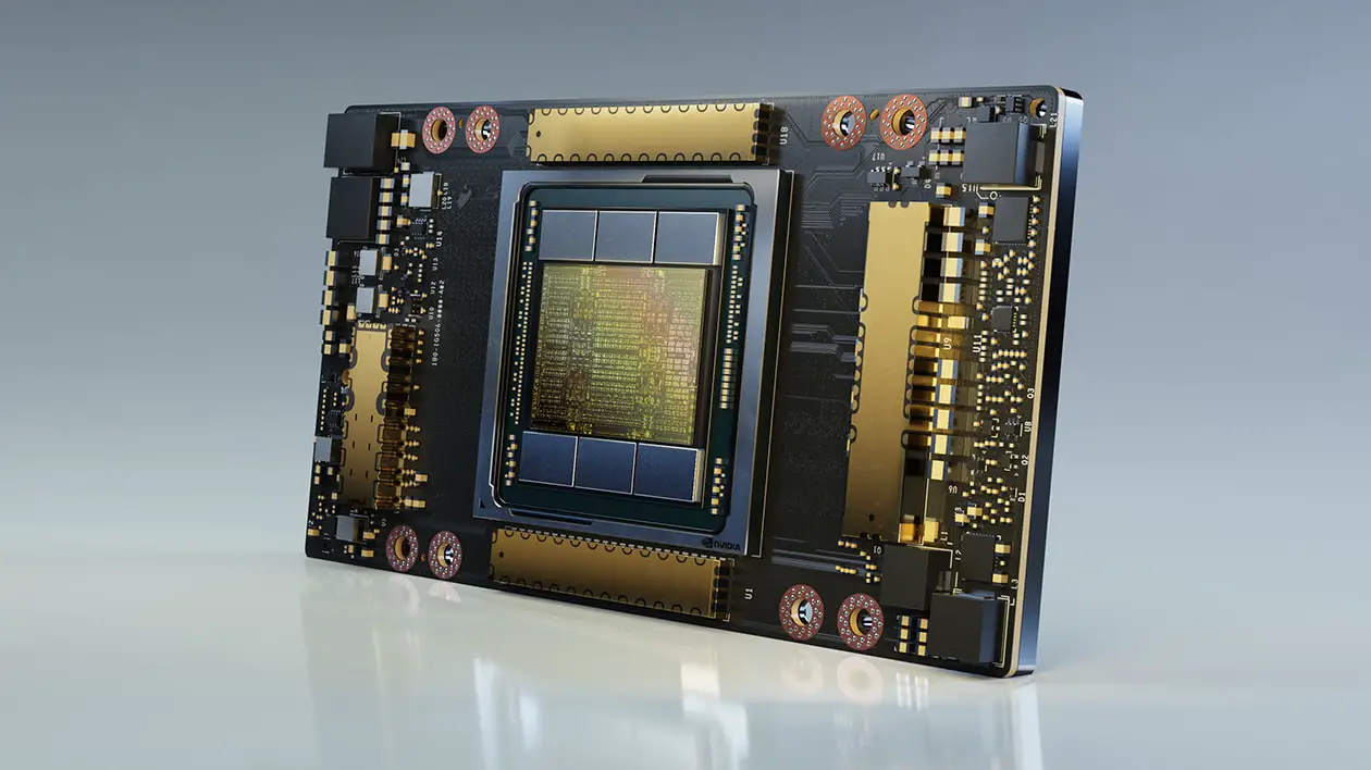
Ampere is introduced as part of the GA100 graphics circuit which is used for data center calculations. GA100 is manufactured on TSMC’s 7-nanometer technology, which according to the company has been optimized for Nvidia’s needs, but exactly what this optimization consists of is not explained in detail. The graphics circuit consists of a total of 8,192 CUDA cores for FP32 calculations, 4,096 cores for FP64 calculations and 512 Tensor cores.
Specifications: Ampere 100
Property | A100 | V100 | P100 |
|---|---|---|---|
Architecture | Ampere | Time | Pascal |
CUDA cores | 6 912 | 5 120 | 3 584 |
Boost frequency | ~ 1,41 GHz | 1 530 MHz | 1 480 MHz |
Memory frequency | 2,4 Gbps HBM2 | 1,75 Gbps HBM2 | 1,4 Gbps HBM2 |
Memory bus | 5 120 bits | 4,096 bits | 4,096 bits |
Memory bandwidth | 1.54 TB / s | 0.9 TB / s | 0.72 TB / s |
Graphics memory | 40 GB | 16 GB/32 GB | 16 GB |
Single precision | 19,5 TFLOP/s | 15,7 TFLOP/s | 10,6 TFLOP/s |
Double precision | 9,7 TFLOP/s | 7,8 TFLOP/s | 5,3 TFLOP/s |
INT8-Tensor | 624 TOP/s | Missing | Missing |
FP16-Tensor | 312 TFLOP/s | 125 TFLOP/s | Missing |
TF32-Tensor | 156 TFLOP/s | Missing | Missing |
Communication link | Nvlink 3 | Nvlink 2 | Nvlink 1 |
Graphics circuit | A100 | GV100 | GP100 |
Transistorantal | 54.2 billion | 21.1 billion | 15.3 billion |
TDP | 400 W | 300 W/350 W | 300 W |
Manufacturing technology | TSMC 7nm | TSMC 12nm FFN | TSMC 16nm FinFET |
Interface | SXM4 | SXM2/SXM3 | SXM |
The computing devices can be shared with a total of 48 GB of HBM2 memory that connects over a 6,144-bit memory bus. The size of the circuit ends up at a massive 826 mm², an area that houses 54 billion transistors. GA100 introduces, among other things, third-generation Tensor cores for artificial intelligence and machine learning calculations.
With Ampere, Nvidia introduces a new floating point calculation format called Tensor Float32 (TF32). The advantage of the Tensor Float32 is that the format combines the scope of the FP32 with the precision obtained with the FP16. The format can also accumulate floating point calculations from FP16 to FP32, which means that developers are not forced to change the code to be able to use Tensor Float32.
This will, among other things, provide twice as fast execution of floating point calculations spread over small parts. Overall, the capacity of FP8 calculations exceeds the capacity of the Volta architecture by 20 ×. A100 applies a 3D packaging where both graphics circuits and memory circuits are placed on the same substrate. The memory circuits are of the HBM2 type, which through the direct connection to the graphics circuits gives a total bandwidth of 1.6 TB / s.
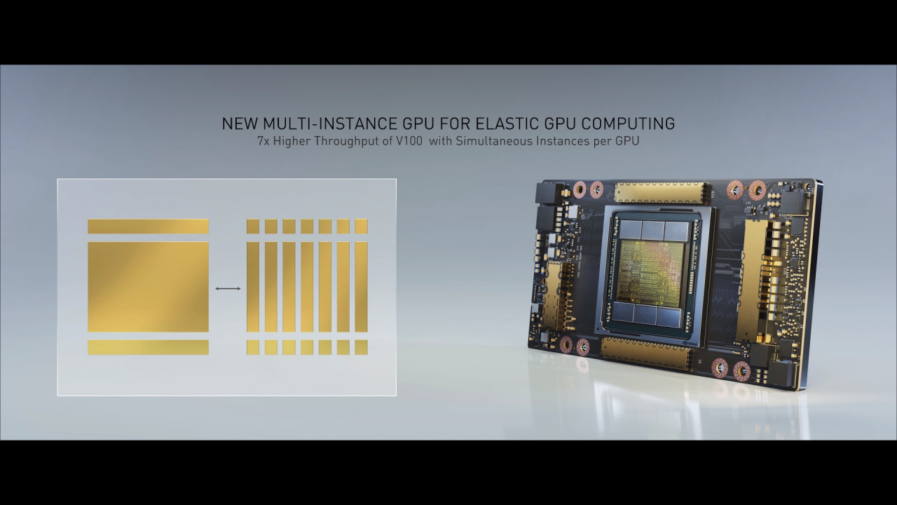
Ampere also introduces a new feature called MIG, an abbreviation for Multi-Instance GPU. It’s about the ability to turn an individual graphics card into several. With A100, this means that a single graphics card can scale up to seven graphics cards that can act independently of each other.
Nvidia likens this to the fact that the company’s previous architectures have been as powerful as a spaceship, but that this spaceship can do nothing else while carrying its massive cargo. With Ampere and MIG, developers can instead divide this cargo into smaller parts and let the spaceships “lift” as soon as the cargo is ready to be delivered.
The function can also be used to divide the computing resources between different users, so that a single A100 graphics card can be distributed between seven different developers. It can be used to let different groups of developers rent a powerful part of an A100, which means that its computational resources are not lost if an individual user does not use its full capacity.
MIG is the basis for Nvidia’s ability to scale up calculations in data centers, from fewer heavy applications to a larger number of small applications. In terms of artificial intelligence calculations, the Ampere delivers six times better performance compared to the Volta-based predecessor V100, to only 75 percent more transistors. In terms of analysis capability (Inference), the A100 is seven times faster than the V100, something Nvidia demonstrates with voice recognition.
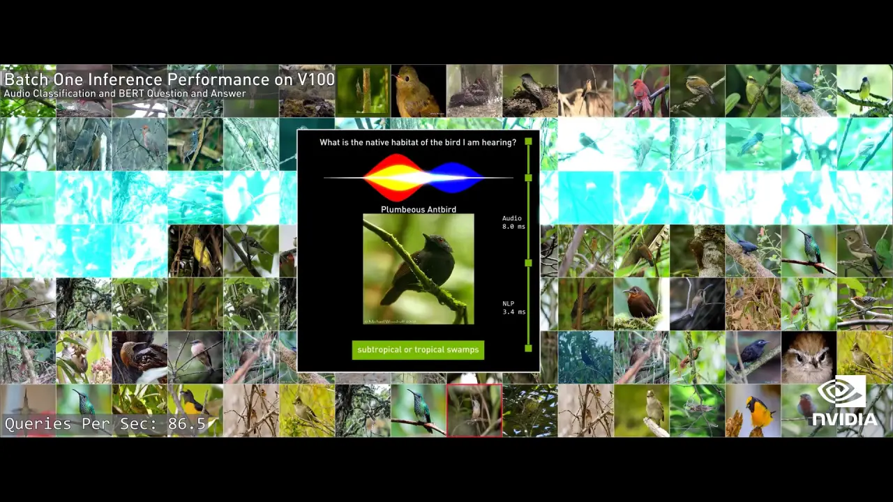
However, voice recognition is not used on human numbers but sounds from birds. By analyzing the chirping of birds, the A100 system determines where in the world the birds are domiciled, where the system delivers responses in just 3.4 milliseconds by performing about 80 requests per second. However, this is accomplished on one MIG device, and when the same test is performed on all seven MIG devices, over 540 requests are performed per second.
The first graphics card to apply the GA100 circuit is called the Tesla A100, which scales down the full capacity of the GA100. This means that only 108 of the complete circuit’s 128 SM units are represented, which also means a total of 6,912 FP32 cores, 3,456 FP64 cores and 432 Tensor cores. The graphics card makes an entrance in the integrated computer system Nvidia DGX A100, which offers a total of 5 petaflops computing power.
The system consists of eight Tesla A100 graphics cards which communicate with dual AMD Rome processors with 64 cores each. The system’s storage is managed by a 15 TB NVME-connected SSD that communicates over PCI Express 4.0. The DGX A100 is primarily intended for use in data centers for the calculation of scientific data and artificial intelligence.
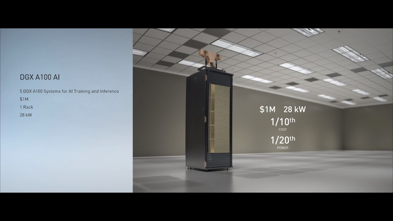
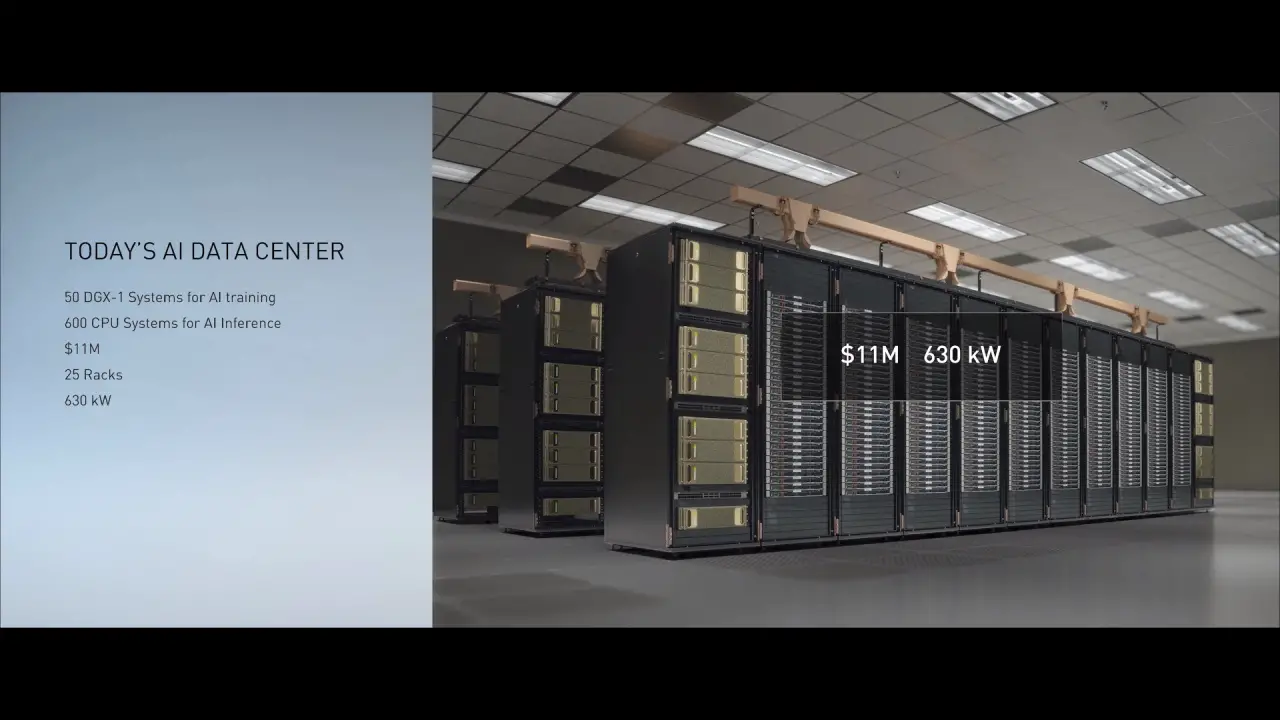
Nvidia announces that the DGX A100 will allow the company to bake enough performance into a server system with a cost of 1 million USD, which with traditional systems would cost up to 11 million USD. A server system based on the DGX A100 combines several applications in one, with an energy consumption of 28 kW. When Nvidia compares this with the energy consumption of previous server systems where different systems work with different areas of use, these amount to a total of 630 kW.
The Nvidia DGX A100 is available for purchase now at the modest price tag of 199,000 USD, corresponding to approximately SEK 2.5 million including VAT.
Related posts:
 Review & Test: Video card Gigabyte GeForce RTX 3060 Ti Gaming OC Pro
  AMD Radeon RX 5600 XT VS GTX 1660 Ti and RTX 2060: Review| Set-up| Hashrate
  Review of the KFA2 GeForce RTX 3060 Ti Core video card
  GIGABYTE GeForce RTX 3090 Gaming OC video card: Review| Specs | Set-up|
  INNO3D GeForce RTX 3090 iCHILL X4 video card review: Test | Config | Hashrate
  ROG Strix GeForce RTX 3070 OC Review: Test | Specs | Hashrate