When Nvidia and AMD took the step from TSMC’s 28 nanometers, they went their separate ways for the first time in several years. Nvidia remained loyal as a customer at TSMC and switched to the new 16-nanometer technology, while AMD broke patterns and began manufacturing 14-nanometer graphics circuits at Globalfoundries and Samsung.
A financial report from Nvidia in the spring of 2015 has previously revealed that the company will lease the production of circuits to Samsung, but not if it was about Tegra or Geforce. During the late summer, this was followed by a report from Chosun Biz, which reported that Samsung had won a contract for graphics circuits, primarily based on the current architecture Pascal.
According to sources at German 3DCenter, the GP107 will be the first graphics circuit from Nvidia to be manufactured by Samsung. The manufacturing technology will be 14 nanometers and provided that the data is correct, this means that the graphics generation Pascal is manufactured on different technologies, as previously GP106, GP104, GP102 and GP100 are produced by TSMC with its competing 16-nanometer technology.
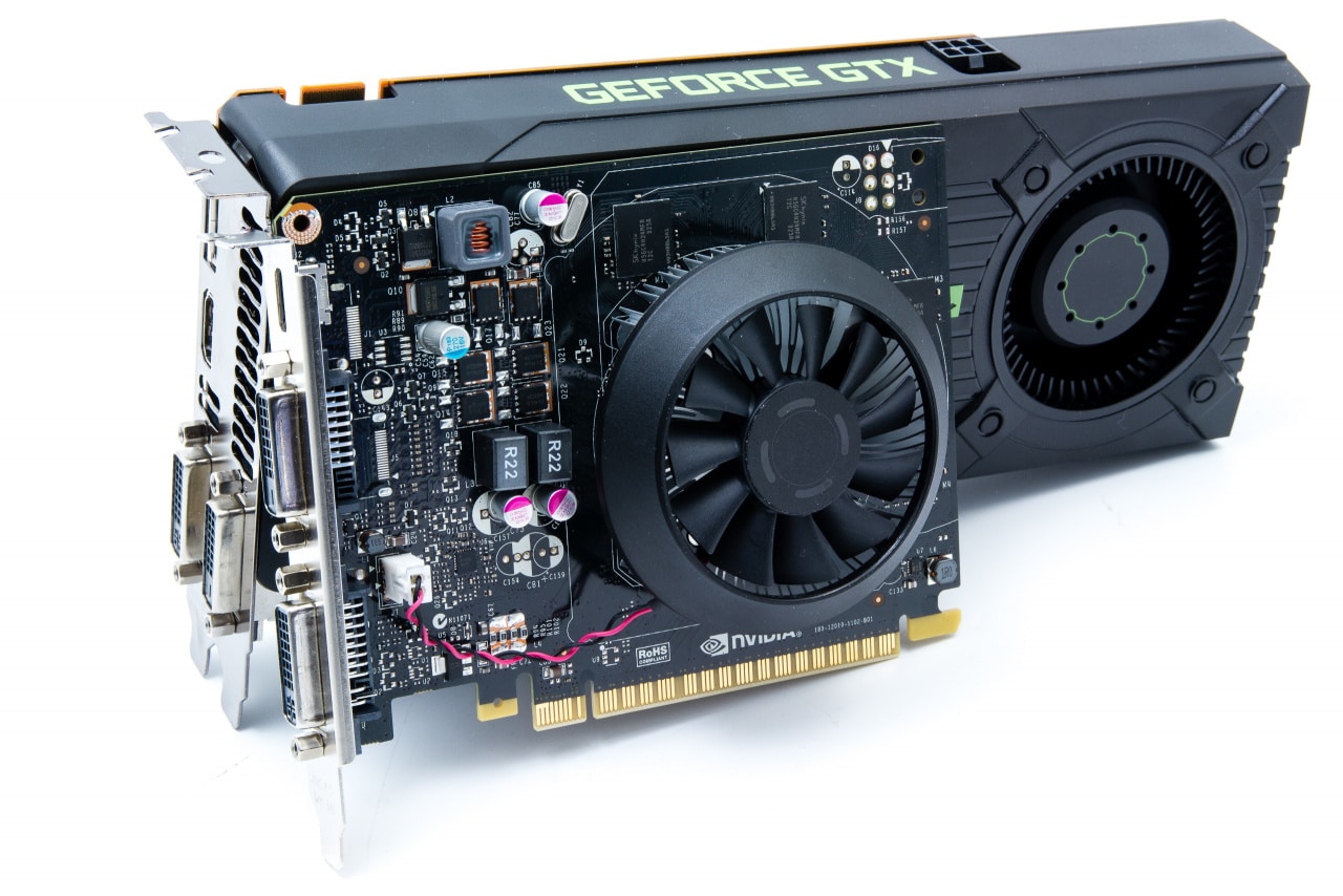
Specifications: GTX 1050 Ti and GTX 1050
GTX 1050 Ti | GTX 1050 | GTX 750 Ti | GTX 750 | |
|---|---|---|---|---|
Technical | 16 nm | 16 nm | 28 nm | 28 nm |
Circuit | GP107 | GP107 | GM107 | GM107 |
Architecture | Pascal | Pascal | Maxwell | Maxwell |
CUDA cores | 768 st. | 640 st. | 640 st. | 512 st. |
Texture units | 48 st. | 40 st. | 40 st. | 32 st. |
Raster units | 32 st. | 32 st. | 16 st. | 16 st. |
Clock frequency | 1 290 MHz | 1 354 MHz | 1 020 MHz | 1 020 MHz |
GPU Boost | 1 382 MHz | 1 455 MHz | 1 085 MHz | 1 085 MHz |
Computational power | 2 123 GFLOPS | 1 862 GFLOPS | 1 389 GFLOPS | 1 111 GFLOPS |
Memory bus | 128-bit | 128-bit | 128-bit | 128-bit |
Memory amount | 4 GB GDDR5 | 2 GB GDDR5 | 4/2 GB GDDR5 | 2 GB GDDR5 |
Memory frequency | 7 000 MHz | ? | 5 400 MHz | 5 000 MHz |
Memory bandwidth | 112 GB/s | ? | 86,4 GB/s | 80 GB/s |
Power supply | – | – | – | – |
TDP | 75 W | 75 W | 60 W | 55 W |
The graphics circuit comes with 768 CUDA cores, 48 texture units, 32 raster units and a 128-bit memory bus. This will house two new graphics cards; Geforce GTX 1050 Ti and GTX 1050, of which the latter gets a scaled-down variant of GP107 with only 640 CUDA cores and 40 texture units. This includes 4 GB GDDR5 for GTX 1050 Ti and 2 GB for GTX 1050.
Measured by Pascal, the graphics cards have relatively low clock speeds of 1,382 and 1,455 MHz for the Geforce GTX 1050 Ti and GTX 1050, respectively, which is still 116-189 MHz higher than the maximum 1,266 MHz for AMD’s Radeon RX 480 manufactured the same manufacturing technology.
According to the report, the low clock frequencies should not be due to any limitation in manufacturing technology. The reason should instead be a conscious design choice from Nvidia who wants to dot 75 W TDP and thus be able to drive the graphics cards without an extra 6-pin PCI Express connector. This could mean that both graphics cards get good margins for overclocking.
The launch of the Geforce GTX 1050 Ti and GTX 1050 is expected to take place in October with recommended prices of 149 and 119 dollars, corresponding to approximately SEK 1,300 and 1,600, respectively, including VAT.
Related posts:
 Review & Test: Video card Gigabyte GeForce RTX 3060 Ti Gaming OC Pro
  AMD Radeon RX 5600 XT VS GTX 1660 Ti and RTX 2060: Review| Set-up| Hashrate
  Review of the KFA2 GeForce RTX 3060 Ti Core video card
 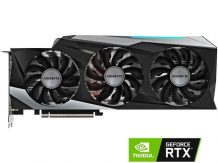 GIGABYTE GeForce RTX 3090 Gaming OC video card: Review| Specs | Set-up|
  INNO3D GeForce RTX 3090 iCHILL X4 video card review: Test | Config | Hashrate
 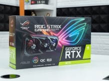 ROG Strix GeForce RTX 3070 OC Review: Test | Specs | Hashrate