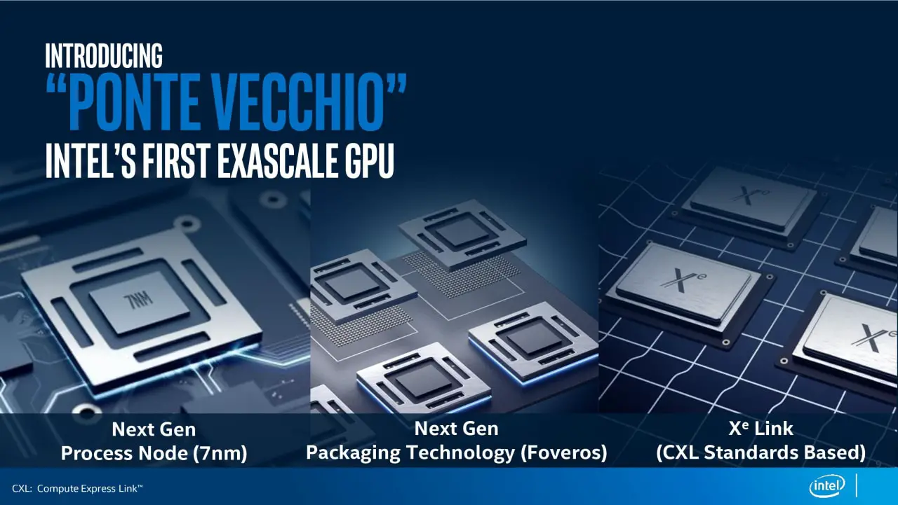
Just a few days ago, the first details of Intel’s first product made at 7 nanometers were found out. It will be a graphics circuit called “Ponte Vecchio” and now the processor giant is going out with official details, both about this but also about the Xe series of graphics cards in general.
Intel has previously said that the Xe graphics cards will have special adaptations for different market segments. It now appears that it will be a common architecture that is shared by everything from integrated graphics circuits to graphics cards and data centers, but that the architecture is branched into three segments where the functions differ.
The first will be Xe LP, where the latter is an abbreviation for Low Power. It is the variant that can be expected to be by far the most common, as it will be integrated with future processors such as the upcoming Tiger Lake. The Xe LP graphics components should scale between 5 and 20 watts, but according to Intel could also be turned up to around 50 watts before the energy efficiency decreases too much.
The second variant is Xe HP (High Performance? / Editor’s note) which is the next step up the stairs. This should be used for Intel’s dedicated graphics cards and should thus scale up to around 250-300 watts. The target group is from personal computers to workstations and data centers.
Initially, Intel only planned to segment its graphics architectures into Xe LP and Xe HP. The company later saw an opportunity to scale up to a third variant – Xe HPC, short for High-Performance Computing. In today’s context, this can almost be compared to Nvidia’s Tesla series, where the graphics circuits are often tailored variants for the area and come with special additions such as greatly improved performance when calculating double precision (FP64) compared to the consumer variants. Focus with Xe HPC are massive data centers in the Exaskala class.
Intel’s first circuit of 7 nanometers will be a graphics circuit according to the recipe Xe HPC and will be named “Ponte Vecchio”. This will not be a monolithic solution but will be based on a number of different technologies that join several circuits. One of Intel’s illustrations clearly shows no less than eight graphics circuits, or chiplet, which sits on a substrate.
One of the technologies is the Embedded Multi-Die Interconnect Bridge (EMIB), which saw the light of day in early 2018 with Kaby Lake-G as combined processor cores, a Radeon graphics circuit and HBM2 memory on the same substrate. The other technology is fresh Foveros, which involves stacking circuits on top of each other.
► Intel Co-EMIB – chiplet design for future processor generations
Conceptually, Foveros is about taking advantage of the benefits of old and new manufacturing techniques. This is done by manufacturing things like computing devices, the cores of a processor or a graphics part, on the very latest technology, while parts such as cache, memory controls and input / output (I / O) are manufactured on older, more cost-effective technologies. In other words, with the Ponte Vecchio, the Execution Unit (EU) is manufactured at 7 nanometers.
Intel Ponte Vecchio is specifically aimed at data centers and will be the first in the upcoming supercomputer Intel Aurora. Each cluster of Aurora will combine six of these graphics circuits with two processors from the Sapphire Rapids family, succeeding Ice Lake in servers. The various components communicate via the PCI Express 5.0-based interface Compute Express Link (CXL) and the OneAPI programming model.
The launch of the Ponte Vecchio will take place in 2021 together with Intel Aurora. Graphics cards for consumers made of 7 nanometers are not expected to appear until 2022.
Source: Anandtech
More reading about Intel’s graphics series Xe and 7 nanometers:
Related posts:
 Review & Test: Video card Gigabyte GeForce RTX 3060 Ti Gaming OC Pro
  AMD Radeon RX 5600 XT VS GTX 1660 Ti and RTX 2060: Review| Set-up| Hashrate
  Review of the KFA2 GeForce RTX 3060 Ti Core video card
  GIGABYTE GeForce RTX 3090 Gaming OC video card: Review| Specs | Set-up|
  INNO3D GeForce RTX 3090 iCHILL X4 video card review: Test | Config | Hashrate
  ROG Strix GeForce RTX 3070 OC Review: Test | Specs | Hashrate