In the summer of 2008, the GDDR5 memory standard was introduced, which has since gradually become the standard for most graphics cards from AMD and Nvidia. Now the technology is about to reach the end of the road, as further advancement in clock frequencies and thus memory bandwidth is expected to be difficult to achieve.
It is therefore beginning to be time for a generational change and the next step for graphics cards may be High Bandwidth Memory (HBM), a memory technology developed by SK Hynix. The basis of the technology is stacked memory according to the concept through-silicon via (TSV), which means that memory circuits are produced with physical holes filled with conductive materials, which create vertical conductor paths when the circuits are joined.
The advantage of this method is that lower voltage is required to send signals between the circuits, which results in lower power consumption and thus also room for higher performance. In the first generation HBM memory, four circuits are stacked on top of each other, each with two 128-bit IO connectors, for a massive width of as much as 1,024 bits per memory capsule.
SK Hynix now announces that HBM will begin mass production during the first quarter of 2015. In addition to the wide IO width, the capacity is 8 Gb (1 GB) with a voltage of 1.2 V and the clock frequency 1,000 MHz, which means a memory bandwidth of 128 GB / s . However, it is possible that an even faster version of 1,250 MHz is on the doorstep.
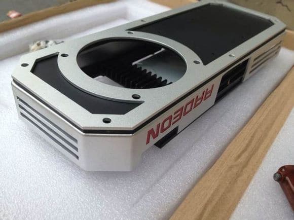
Earlier in November, what is believed to be AMD’s upcoming graphics card was listed in the top performance class in the performance database for the test suite Sisoft Sandra. There appeared a 4,096 bit memory bus with video memory of 1.25 GHz or 1,250 MHz. Provided that the information is correct, four of SK Hynix’s HBM capsules would mean a total of 4 GB of HBM memory with a bandwidth of a record high 640 GB / s.
However, the performance database is not the only one that indicates that the new memory type can be housed in AMD’s upcoming flagship “Radeon R9 390X” with the graphics processor “Fiji”. It is no secret that the processor maker has collaborated with SK Hynix on the memory standard, which indicates that HBM should reasonably be used in any of the company’s future products.
In addition to the new memory type, AMD Fiji is expected to have a full 4,096 stream processors. That’s a little more than 45 percent more than the 2,816 units housed in Hawaii, which is the graphics processor used in the Radeon R9 290, 290X and 295X2.
Source: Kitguru.
Related posts:
 Review & Test: Video card Gigabyte GeForce RTX 3060 Ti Gaming OC Pro
  AMD Radeon RX 5600 XT VS GTX 1660 Ti and RTX 2060: Review| Set-up| Hashrate
  Review of the KFA2 GeForce RTX 3060 Ti Core video card
  GIGABYTE GeForce RTX 3090 Gaming OC video card: Review| Specs | Set-up|
  INNO3D GeForce RTX 3090 iCHILL X4 video card review: Test | Config | Hashrate
  ROG Strix GeForce RTX 3070 OC Review: Test | Specs | Hashrate