Modification and extreme overclocking: NVIDIA GeForce FX 5900 Ultra versus ATI RADEON 9800 Pro
It’s not a secret for anyone interested that the R360 and NV38 chips from ATI and NVIDIA are nothing more than overclocked versions of their predecessors, NV35 (NVIDIA GeForce FX 5900 Ultra) and R350 (ATI RADEON 9800 Pro). Moreover, if in the case of NVIDIA the relatively recently released chip underwent “official overclocking”, then ATI still, in fact, only systematically increases the frequencies of the good old R300.
In today’s review, I decided to prepare for the release of NV38 and R360, compare the overclocking potential of NVIDIA GeForce FX 5900 Ultra and ATI RADEON 9800 Pro, and squeeze all the juice out of them, adopting a well-known method – increasing the GPU voltage and video memory.
The test cards were a video card from MSI based on NVIDIA GeForce FX 5900 Ultra included in the NBOX package, and PowerColor R38-C3 based on ATI RADEON 9800 Pro.
First part: MSI NBOX (NVIDIA GeForce FX 5900 Ultra)
Second part: PowerColor R98-C3 (ATI RADEON 9800 Pro)
Third part: Test system, extreme overclocking, testing, conclusion.
MSI NBOX: “Ultra” – во всём!
A video card based on NVIDIA GeForce FX 5900 Ultra is presented in today’s review by MSI with its luxurious NBOX set.
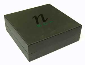
NBOX is stylishly and emphatically laconic – you will not find any beauties or monsters, terminators and other “high-tech” tinsel on the box:
An even more laconic packaging is hidden under the cardboard shell – a black box. You can only guess what is inside by the NBOX logo on the top cover:
Under the cover there is a video card, laid in a mold made of a thick layer of microporous rubber. The video card is kept in it very tightly, but it can be removed calmly even with two fingers – for this, the form has special cutouts:
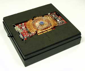
Everything else is in the lower compartment of the box. In order to get to it, you need to lift the compartment with the video card – on the left in the photo you can see a strap made especially for this. When lifting the compartment with the board, a characteristic sound is heard – this is the “Velcro” fastener that held it in the closed position for greater reliability.
So what’s in the box? Let’s see:
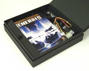
The first thing that catches your eye is an optical USB mouse with the MSI logo and a mat with the Command & Conquer Generals logo:

I’ll say right away: the MSI mouse with aluminum keys and blue backlit wheel looks, of course, stylish, but it will not be used for its intended purpose, that is, in games, most likely, it will not be – it is not as convenient as the specially designed tools. meticulously selected by gamers especially for themselves. But you can’t find fault with the rug – it is thin, comfortable, with a special coating that prevents sliding on the table – in general, what you need.
Moving on. Further – disks with drivers and utilities from MSI and three full-fledged game hits: Unreal 2, Battlefield 1942 and Command & Conquer Generals, each of which is accompanied by a paper “course for a young soldier”:

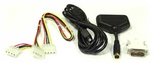
Finally, the package includes a set of cables and adapters: an S-Video cable, an adapter from a combined video input-video output connector to 2 RCA and 2 S-Video connectors, a DVI-> D-Sub adapter and a cable for connecting additional power:
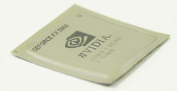
Now it’s time to tell you more about the MSI graphics card itself. NBOX is based on the standard FX5900U-VTD256 model based on NVIDIA GeForce FX 5900 Ultra:
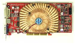
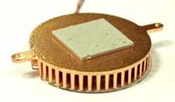
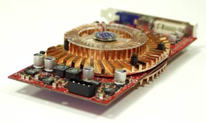
The cooler located on the front side of the board covers both the graphics core and the video memory chips at once. The air sucked in by the fan diverges in all directions along the radiator fins – they are located radially. Thermal grease is used to improve thermal contact between the heatsink and the cooled chips:
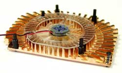
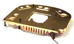
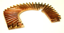
For such “monolithic” coolers that cover both the graphics core and the video memory, it is difficult to ensure good contact with all cooled chips, but on our video card the cooler on the front side was almost perfect for all the chips. The cooler located on the back side of the board consists of two parts: one is designed to remove heat from the video memory chips, and the other from the board surface under the GPU. Contact with the board surface is made through a thick elastic heat-conducting pad:
I doubt this cooler contributes much to GPU cooling. However, it is good because it produces an air flow that blows over the fins of the heatsink installed on the video memory chips:
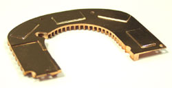
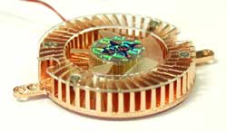
Blowing on this heatsink would be more useful if it did not just press against the video memory chips, but had at least a small amount of thermal paste in the places of contact with the chips.
However, this is nit-picking: the board works stably at standard frequencies, but for overclocking you can use thermal paste :). And the last point regarding the cooling system: all the radiators on the video card only look as if they are made of copper. In fact, they are made of aluminum alloy – on a small notch, which I made with an ordinary paper cutter, metal of a different color is visible:
The video card is equipped with standard D-Sub, DVI-I connectors and a combined video input-video output connector:
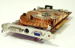
On the opposite side of the board, like all video cards based on NVIDIA GeForce FX 5900 Ultra, there is a connector for connecting an additional power supply:
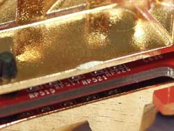
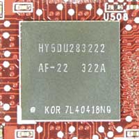
The basis of the board is an NVIDIA GeForce FX 5900 Ultra graphics processor and 256 MB of video memory in Hynix chips with a cycle time of 2.2 ns:
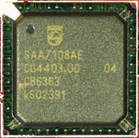
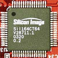
The clock speeds in 3D mode are by default equal to the standard 450 MHz for the graphics core and 850 (425 DDR) MHz for the video memory. The TV signal shaping for video output is provided by the integrated GPU unit, and the decoding is provided by the popular SAA7108 chip from Philips. The digital signal transmission to the DVI connector is provided by the Sil164CT64 chip from Silicon Image:
So, the FX5900U-VTD256 from MSI, which is part of the NBOX, is a solid video card based on NVIDIA GeForce FX 5900 Ultra, made according to the reference design. Among other motherboards, it is distinguished by an unusual appearance, a high-quality cooling system and a very low noise level – its coolers are practically inaudible against the background of other system noises.
There is only one thing I can say about MSI’s NBOX package: this is how “top-end” gaming video cards should be equipped and designed. For a few hundred dollars for a graphics card, you want more than a standard board, a pair of cables, and a driver CD packed in a lurid cardboard box, right?
At the end of my initial acquaintance with NBOX, all I had to do was mention the board’s overclocking potential. The maximum frequencies at which the FX5900U-VTD256 mainboard worked steadily were 570 MHz for the GPU and 950 (475 DDR) MHz for the video memory.
The result is not bad, but not too impressive. But this is just the beginning! .. 🙂
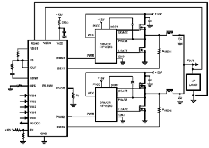
GPU Power Stabilizer Features
The GPU power regulator on the board is based on the ISL6569 chip from Intersil . The ISL6569 chip is a “highly intelligent” pulse-width controller for a two-phase switching power regulator with protection against overvoltage and current in the load, “soft turn-on”, balancing of currents in channels, temperature stability of the output voltage
Well, this is the first time I’ve come across two-phase power supply regulators on gaming video cards – they are usually used on motherboards in power supply regulators of powerful processors.
It looks like the NVIDIA GeForce FX 5900 Ultra chip really has such a high consumption and voltage stability requirements that from now on, two-phase power stabilizers have appeared on video cards. However, this is not the most interesting thing …
The output voltage of the stabilizer is set by feeding a binary code to the DAC inputs of the microcircuit:
Setting the output voltage with a binary code is no longer a novelty, but a distinctive feature of the ISL6569 is the ability to change the output voltage on the fly – when the input data changes, the controller smoothly raises or lowers the output voltage of the stabilizer to a new level set by the new code.
It is obvious that such a “smart” regulator with a variable output voltage is installed on the board for a reason. Observing the voltage of the GPU, I found confirmation of my guesses. It turned out that the supply voltage of the NVIDIA GeForce FX 5900 Ultra does change in different modes:
At the stage of computer startup, until the Windows XP graphical shell and the video card driver are loaded, the supply voltage is 1.1V .
Immediately after loading the driver, the core voltage rises to 1.2V . It remains unchanged in any 2D application.
When starting any 3D application, the voltage rises even higher, to 1.4V, and drops to 1.2V only when switching back to 2D mode.
So, NVIDIA engineers have provided video cards based on the GeForce FX 5900 Ultra and Detonator drivers with the ability to control the voltage of the GPU. If we recall that the frequencies of the core and video memory in 3D mode increase relative to frequencies in 2D, then the question arises: why does the chip supply voltage rise higher when switching to 3D mode? In order for the core to work at higher frequencies more steadily?
Unlikely. Most likely, this situation should be reversed: in 2D mode, the GPU voltage drops relative to the voltage in 3D mode. At the same time, the clock frequencies are lowered. In this case, there are no questions: this was done in order to reduce power consumption and heat dissipation of the board at a time when it is not required to demonstrate miracles of performance.
Increasing the voltage of the graphics core
In order to increase the voltage of the graphics core, as it turned out, it would be enough to change the part of the driver code that is responsible for setting the voltage in 3D mode, or to program it yourself. Let’s hope that soon there will be utilities that will allow you to change the voltage supply of NVIDIA GeForce FX 5900/5900 Ultra, but now we will have to look for a hardware method – I don’t understand the “internals” of drivers and other assemblers at this level :). The board’s power regulator is excellent for outside interference: the ISL6569 microcircuit has a special OFS input connected to a current source and a divider. When connecting a resistor between the OFS input and the common wire, you can raise the output voltage of the stabilizer relative to what is set by the binary code at the DAC input:
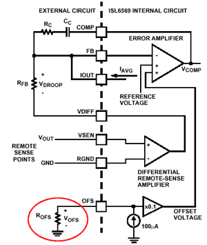
The voltage offset value when connecting a resistor with resistance R will be equal to (100μA * R) / 10 .
On the MSI video card, the OFS pin of the ISL6569 is connected to the common wire through a chain of zero-resistance resistors, so it is very easy to increase the voltage, you just need to replace one of the links in this chain with a resistor with the required resistance. For convenience, I summed up the wires instead of the resistor:
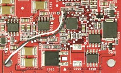
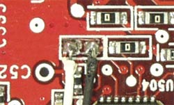
… to which, in turn, I soldered an ordinary variable resistor with a nominal value of 33 kOhm:
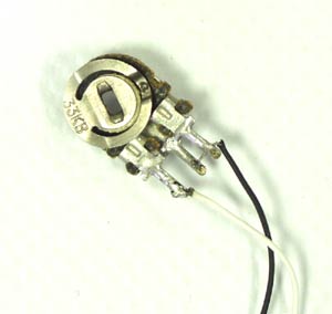
In extreme overclocking, I settled on the resistance of this resistor of about 30 kOhm , as a result of which the GPU voltage in 3D mode was 1.69V , that is, it increased by 0.29V .
Do not forget that the voltage offset value does not change with any input data to the ISL6569 DAC, so the graphics core voltage rises in all modes. Accordingly, the heat dissipation also increases, which means that the graphics processor needs adequate cooling. About cooling and the achieved frequencies of the GPU – a little later, and now – about my failures with extreme overclocking of video memory …
Increasing the supply voltage of the video memory
Having dealt with the power supply stabilizers of the video memory microcircuits, I immediately raised the supply voltage of the internal circuits and input / output buffers (VDD and VDDQ) by 0.2V and decided to check how much the overclocking potential of the video memory microcircuits had increased.
The results of the experiments upset me: the maximum video memory frequency, at which the board worked stably, remained the same after increasing the supply voltage: 950 (475DDR) MHz .
Having increased the supply voltage by another 0.2V, I again began to experiment with overclocking the memory. The result remains the same again: 950 MHz..
I. began to increase the voltages even higher, then, on the contrary, lower them relative to the nominal, then vary VDD and VDDQ separately, changing the voltage ratio, then experiment with a heat chamber and minus temperatures, but the maximum video memory frequency during overclocking remained unchanged – 950 MHz. In the end, I gave up and gave up on raising the voltage supply of the video memory. Apparently, 950 MHz is the limit for the reference design of NVIDIA GeForce FX 5900 Ultra and video memory chips from Hynix. So, it’s time to start testing. The board is ready:
… and all that remains is to change the cooling system for the graphics core and video memory chips.
Refinement of the cooling system
The NVIDIA GeForce FX 5900 Ultra graphics processor has a metal cover. This cover, covering the crystal, is made of copper, and in addition to the main task of protecting the core from chips, it distributes heat over the contact surface with the heatsink. However, in order to achieve maximum overclocking results, it is better to get rid of any “intermediaries” when transferring heat from the chip to the heatsink. So I removed the cover from the GPU:
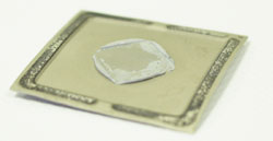
This operation was done with a sharp paper cutter. For those who, disregarding the guarantee, decide on such an experiment, I strongly recommend doing it as carefully as possible – there are “gentle” current-carrying paths in the multilayer substrate of the chip, which are very easy to damage with one careless movement.
So, the graphics processor NVIDIA GeForce FX 5900 Ultra “no tie”:
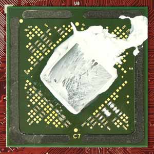
The white thermal paste in the photo is KTP-8, which I used to improve the thermal contact between the crystal and the water block of the cooling system.
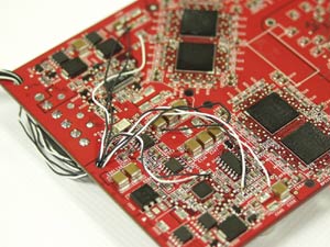
To remove heat from the GPU, I used the Thermaltake Aquarius II water cooling system as standard. Due to the installation of the water block, we had to abandon the standard cooler, which immediately covers the graphics processor and video memory chips. On them I installed heatsinks from a motherboard based on NVIDIA GeForce FX 5900 Ultra, made according to the reference design.
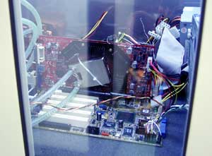
The assembled test system with a video card from MSI began to look like this:
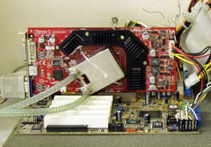
To increase the overclocking potential of the video card, the system was placed in a thermal chamber that maintained a temperature of -15 degrees Celsius, where all the tests were carried out:
So, a video card from MSI based on NVIDIA GeForce FX 5900 Ultra is ready for testing. It’s time to prepare a worthy competitor based on the ATI RADEON 9800 PRO for it. First part: MSI NBOX (NVIDIA GeForce FX 5900 Ultra) Second part: PowerColor R98-C3 (ATI RADEON 9800 Pro) Third part: Test system, extreme overclocking, testing, conclusion.
Related posts:
 Bitmain Antminer r4 Review – Benefits Profitability Payback Specification
  Nvidia GTX 1080 ti Hashrate – Review | Overclocking |Ethereum |Profit (sky high)
  Antminer S5 ASIC Hashrate – Review Profitability Payback Period
  Asic Antminer S1 Hashrate – Review | Test| Specs| Pros & Cons | Set-up|
  Miner Baikal Giant x11 – Hashrate|Profitability| Specs
 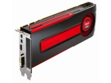 Radeon Hd 7970 Hashrate -Review|Profitability | Specs | Pros and Cons